This thread has been locked.

If you have a related question, please click the "Ask a related question" button in the top right corner. The newly created question will be automatically linked to this question.

DAC81408: Schematic review support

Part Number: DAC81408


Hi

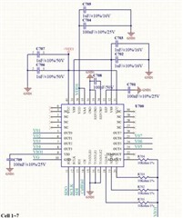
My customer Simplo is using DAC81408 for the battery test equipment product. 

May I have your support to review the schematic (Please find it in the attachment) to see if you have any suggestion? Thank you. 

Here is the project info.  

  • End customer: SMP
  • Application: Battery test equipment
  • MP schedule: 2022Q4
  • Forecast: 1k

  • Hi,

    If you are asking for schematic review, please attach a pdf of the same or high res image. Some of the net names are not visible. For example:  VSS is connected to ground through capacitor, but there is no net name.

    Why pin 10 is not grounded? Its named as net VG, is it connected somewhere?

    Regards,

    AK

  • Hi AK, 

    Thanks for the support. Yes, I am asking the schematic review support. 

    The schematic in pdf format will be encrypted at my side side, so that's why they share the images with me. 

    I have asked them to regenerate the images. Please find it in the attachment.

    Stack DAC81408.zip

    Thanks, 

    Jack 

  • Hi,

    Please see my comments below.

    1. Pin 10 should be grounded, I am not seeing that in the schematics (Cell 1-7)

    2. Do you plan to use device for unipolar or bipolar outputs? If its unipolar VSS should be connected to GND. I am not seeing any net names for this pin in the schematics. This pin looks as good as floating with a cap connected. ( You need to have an option to GND or give -ve supply to this pin)

    3. Does GND1 and GND2 connects somewhere on the board? What is the need for this separate GND?

    Regards,

    AK

  • Hi AK, 

    Thanks for the comments. 

    About the second comment, the design was for unipolar output (0~40V), they followed the EVM design to short 2 VSS first and then connect to GND through two 1uF capacitor. Do you mean they should have the option to connect to GND directly? 

    About the third comment, GND1 and GND2 have two different voltage levels (stack design). It will have two AC/DC adaptors; these two adaptor won't be connected. In order to have the stack design, they connect the second DAC GND to the first DAC cell7's GND. Do you have any suggestion for this type of design? 

    Thanks. 

    Jack

  • AK will take a look at this tomorrow.

  • Hi,

    They should connect VSS to GND if its a unipolar operation. Have that option.

    I understood about the stacked design. Make sure GND node is at appropriate levels without exceeding device limits.

    Thanks,

    AK

  • Hello AK, 

    Thanks for the support. 

    Regarding your second comment " Make sure GND node is at appropriate levels without exceeding device limits.", I would like to double confirm with you. Are you referring the GND voltage (-0.3V to 0.9V)?

    Thanks. 

    Jack

  • Hi,

    Yes, I am referring to -0.3V to 0.9V RFEGND to GND

    Regards,

    AK