- Ask a related questionWhat is a related question?A related question is a question created from another question. When the related question is created, it will be automatically linked to the original question.
Problem Description:
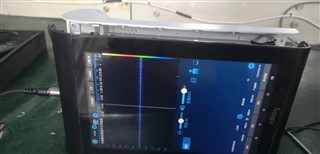
After the temperature of the thermal imager test chip rises by 50 degrees, the input is 0, and the output has noise and serious interference. The output waveform is shown in the attached picture. After the temperature decreases, the output noise disappears and the output waveform is particularly clean. Please help analyze.
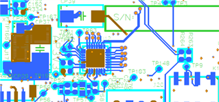
PCB Description:
The analog ground and digital ground of the circuit board are not grounded at a single point. The two grounds are shared. See the attachment for the schematic diagram and some PCB pictures. If there are any good suggestions for PCB layout, you can also provide the following information. thank you!