


Hello,
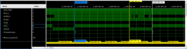
When we used the ADS8671 to acquire data, we were acquiring the amplifier amplified signal, the amplifier output +-12.288V signal, Vref=4.096V.
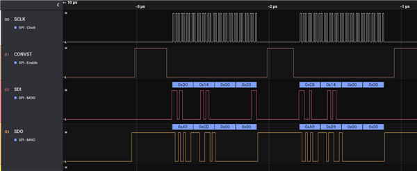
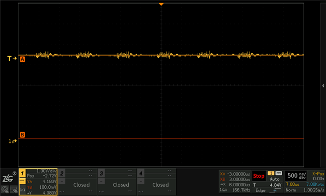
Below is the SPI waveform: adc input voltage range is +-12.288V, Vrefio=4.096V,using the default configuration. But the Vin amplitude decreased 4.5~5.5 times with the output code and LSB equation.
Best regards
Kailyn


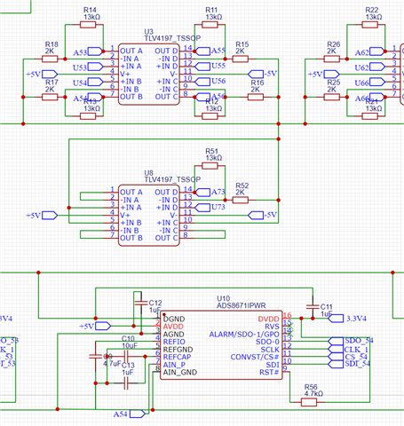
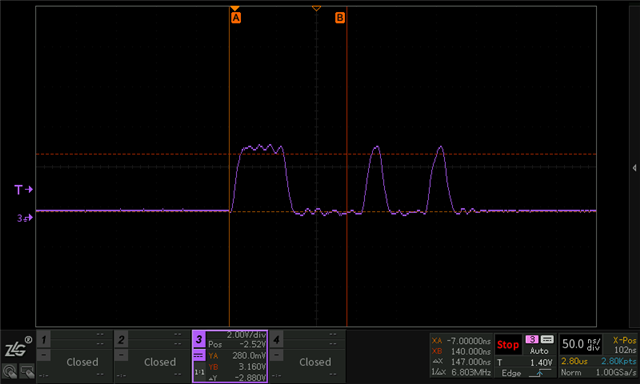
 REFIO
REFIO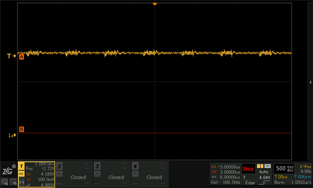 REFCAP
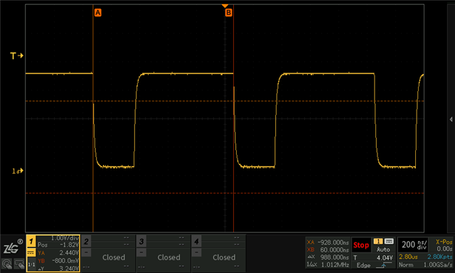 (CS)
(CS)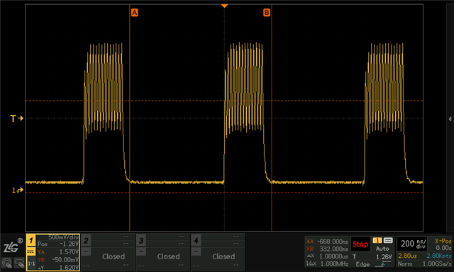 (SCLK)
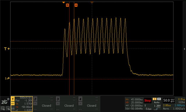 (SCLK)
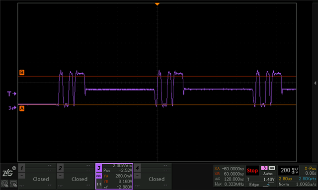 (No
(No 
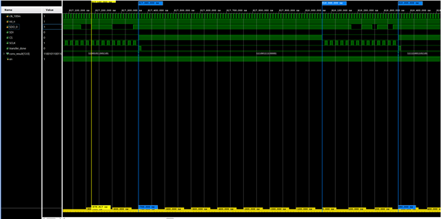
 SDO output with AIN_P input