This thread has been locked.

If you have a related question, please click the "Ask a related question" button in the top right corner. The newly created question will be automatically linked to this question.

ADS131M06: DRDY format and frequency

Part Number: ADS131M06

I appear to be having a problem setting up an ADS131M06. I can read back the registers I set but there appears to be no difference in the output.

I've checked the signal with an oscilloscope to check the edge quality and with a logic analyzer to ensure longer bitstreams are correct. In addition the fact that the readback of the register gives me the same value as the one I wrote it suggests that the writes are performing correctly which provides a secondary check of the signal timing and bit order.

I write a value of 0x3F1E to the CLOCK register which should result in

channels 0-5 enabled

OSR bits set to 7 for an OSR of 16256 and a conversion rate of 250 SPS given my clkin rate of 8.192MHz

PWR bits set to 2 or default high resolution

In addition I write a value of 0x511 to the MODE register which should result in

register and input CRCs disables

reset bit left high

SPI timeout enabled

Most lagging channel controlling *DRDY

*DRDY driven high when no data ready

*DRDY an active low pulse of 4 clkin or ~0.5uS at 8.192MHz clk rate.

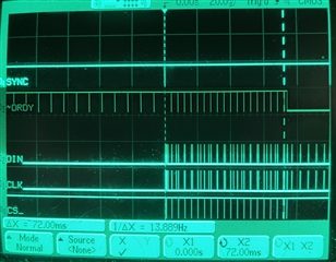
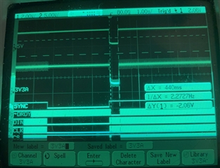
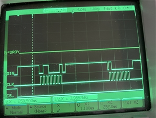
However, I'm seeing a *DRDY rate of 4kHz+ with the signal being mostly low as shown

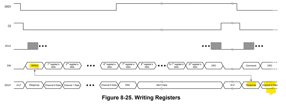
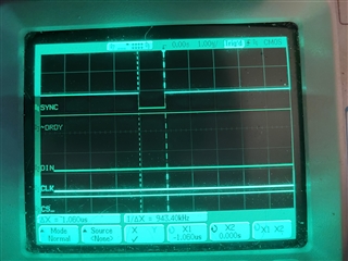
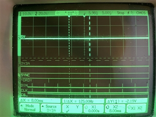
The next shot shows the write sequence for the CLOCK register

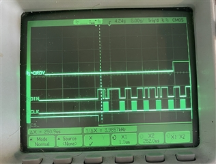
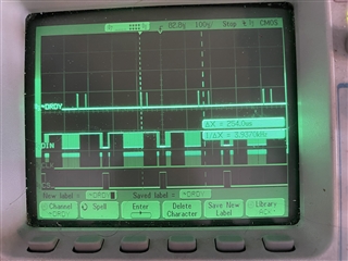
And two images showing the details of that write

first the command

And then the register value

I have the same sequence for the writing of the mode register. I don't think it adds much information though.

I'm sure I'm either missing or misunderstanding something in the datasheet but at this point I don't know what it is. I'd have expected to get a narrow low pulse from the *DRDY line at ~250 - 500Hz given those settings (up to 500 because of internal buffering) but I'm getting a majority low line and at 4kHz. The settings don't seem to affect the behaviour. Any ideas as to what I'm missing?

Robert

  • Hello Robert,

    I'd be curious to see the logic analyzer shots that include DOUT. What does the result of a NULL command give back? When reading for the first time, are you clearing the FIFO by reading twice before the next data transition occurs?

    Let me break down what I am seeing. The first screenshot shows that there's not enough SCLK periods to read out the whole frame before the CS pin goes high again. I assume you're doing a register write. The datasheet shows that the device expects to read all channels to complete the frame. 

    Reading all data on a command ensures "predictable DRDY pin behavior" as shown below from the datasheet:

    The rest of the screenshots only show me that, as you said, signal integrity isn't an issue as I don't see DOUT and any rest of the SPI frame. I agree that if you're able to write and read that value back, then you probably have the format of the command and the timing correct. However, because you are choosing to not read the whole frame you'll need to follow the "collecting data for the first time" where you'll need to clear the FIFO by reading data twice in row before the next data transition comes in.

    In short, I suggest deciding to clear the FIFO and then look at DRDY behavior, or show some screenshots that you're doing that and we debug by taking a look at logic analyzer screenshots and the result of a NULL command.

    Best,

    -Cole

  • There should be enough sclk periods for the data. The screenshot simply doesn't have the resolution to show them. There's a total of 24 8 bit bytes. I have verified that they occur.

    I can get data in, I know about the data buffering but at that frequency from *DRDY, it's simply not possible to keep up.I do perform a synch after setting the clock and mode registers so there shouldn't be any retained data. Indeed I should have 4 mS before the first *DRDY

    I included the higher resolution writes to show I was performing. the write correctly.

    The questions remain

    1. why am I not getting a fixed width low pulse as the data sheet says I should?
    2. why am I getting a 4kHz *DRDY instead of a 250Hz one? (I could understand getting two close to zero followed by a 4mS gap  if the buffer was filling. That's not what I'm seeing though).

    The first question, in particular, bothers me since the data sheet indicates the pulse width should only be 4 clkin wide and that's just 1/2uS which is far from what I'm seeing.

  • Hey Robert,

    Okay, sounds like you get the whole data frame and, to your point, a logic analyzer is better for displaying those sorts of things. I'm still unsure why CS releases between each byte. I'd still like to see them if you have them handy

    For question 2, we'll need to figure this out first and the rest should be easier to debug. I don't have a good answer why the data-rate didn't slow down and follow the OSR setting. 4kSPS is the default so there's some relationship there we need to better understand. Let me talk with the team and see what they think.

    For question 1, is it possible to switch back to logic low instead of negative pulse for DRDY_FMT as a short term debug step to see if DRDY is acting the same? Furthermore, we most likely have to wait until question 2 is fixed if we will run into the FIFO filling up and causing "unpredictable DRDY behavior".

    Also, small note on the FIFO, if you miss two samples in a row, all data is cleared out. Its not really a true FIFO in that respect.

    As always, here's some reference code if you have not seen it before: http://www.ti.com/lit/zip/sbac254 

    Best,

    -Cole

  • The CS isn't releasing between bytes, you are just seeing aliasing in that first picture because the time frame is compressed. I'll get several shots to show it but it gets rather repetitive after the first 6 bytes.

    The default format for *DRDY behaves in the same fashion. I switched format since the *DRDY behaviour would be low while data was ready as I understand the datasheet and I wanted to switch to something that would be guaranteed to follow (at least somewhat) the conversion rate.

    I'll also get a shot of the behaviour immediately after the sync. I do have three converters running, so I'll also concentrate on a single one.

  • Hey Robert,

    No need to grab them if it'll be a pain and the data looks like it isn't copied and pasted (i.e. real channel data).

    At this point, I think we need to reverify your main steps. I do think:

    • Write and read configure registers
    • SYNC to clear FIFO
    • Send NULL or some command to read data

    Is a good set of steps for your application. That being said, we need to verify each of these steps because the waveforms and the procedure seem to contradict each other.

    Let's start with read and write, can you please read ID (reg: 0x0) and see what the response is on the oscilloscope (or logic analyzer)? This will test the read.

    For the write, can you please read the STATUS register and ensure the RESET (bit[10]) is 0b1, write 0b0 to the RESET bit (bit[10]) of MODE, and finally read STATUS again to make sure the RESET bit flipped to 0b0?

    For SYNC, I'd like to see CLK, SYNC, DRDY, and DOUT on an oscilloscope capture to ensure the timing falls within the SYNC but not the RESET criteria.

    And for reading data, I'd like to see the CH0_CFG MUX changed to short the inputs together and then read the output. With the gain and VREF noted, we should be able to check out the offset and see if it falls within spec of the device. 

    I know its kind of tedious but we're at the point where the behavior doesn't make sense but we need to verify our assumptions.

    Best,

    -Cole

  • Cole, sorry for the delay. I did get some measurements. Starting with the pulse width of the sync pulse, I then aimed to see what the timing was immediately after and it revealed something interesting. I specifically reduced to a single A/D to reduce the variables involved as well.

    First the sync pulse

    As you can see, it's a little over 1uS. On expanding the view I found the following

    The first *DRDY pulse arrives 4 mS after the sync as expected and then every 4mS for 18 conversions before falling low for an extended period. After which it resumes at 4kHz.

    It would appear that the IC is resetting. Any suggestions on source? I am going to check both the other ICs on this board and another board to see if the behaviour varies or is consistent.

    Robert

  • Hey Robert,

    That's an interesting find. The SYNC looks correct but it appears the behavior starts as soon as the SPI lines start to release. I'm interested if you could probe at the DVDD pin, and AVDD pin for that matter, just to ensure the supply rails are stable. The fact that the behavior lines up with the first SPI line transition is suspicious.

    The only real way to get RESET on the ADC is through the pin, which doesn't seem to be the case; through a RESET command; or Power On Reset (POR). Out of the 3, the POR seems to most likely. There is also a SPI timeout and reset, which is for communication and not the device itself, but you'd need to wait 4ms for that so I find that unlikely as well.

    Best,

    -Cole

    Edit: clarified SPI

  • Cole, that sent me on a search. Let me bring you up to date.

    After instrumenting the power line I found this behaviour on the 3V3 analog (and the 5V that feeds it)

    The digital 3V3 was fine. Clearly this was an issue. Initially puzzled on the timing, I did track it down to power up sequencing. The power was cycling after the sync. Changing by delaying the setup and sync until after the power rather than rushing headlong into it fixed that issue. As you can see there's a nice steady 125Hz (Half of the 250Hz nominal since at this point I had stopped reading the values to simplify interactions)

    I've been able to add the reading back in and adjust the conversion to what I was initially aiming for. I've also managed to measure the drift of the DRDY between different ICs.

    Thanks for your help

    Robert