This thread has been locked.

If you have a related question, please click the "Ask a related question" button in the top right corner. The newly created question will be automatically linked to this question.

ADS1220: ADC only answers 0xFFFFFF for a period of time

Part Number: ADS1220


Hi,

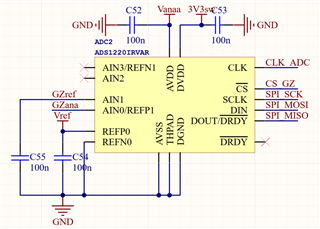
We're using 6 ADS1220 in one of our product. They are all configured identically in continous conversion mode, communicate through the same SPI bus, and are clocked by the same 3MHz signal (CLK pin). The "start" command is sent through SPI with all 6 CS pins activated, then a single DRDY pin is polled to trigger data gathering of all 6 ADCs from an STM32.

We usually don't have any issue, but some samples answer 0xFFFFFF continuously for a period of time.

When this happens, most ADCs work fine, but one (rarely more) only answers 0xFFFFFF when the continous data is read, and also 0xFFFFFF when the configuration registers are read. This situation may continue for a long time, or disappear after a power-off. It may reappear on the same ADC, or another one. Some systems are often faulty, on others it occured once, for most of them never (I don't have a very precise estimate, but I would say <10 samples for 200+ products).

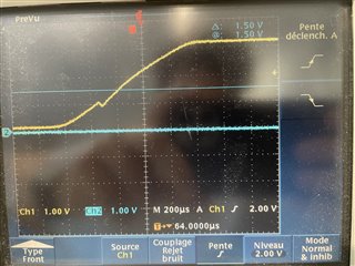
We managed to measure the SPI signal in real time, the MISO line is effectivelly driven high for the time of the CS activation.

We found an implementation error on our side : The external 3MHz clock had a duty cycle of 25% instead of the 40-60%, but since we lack a reliably faulty device we cannot easily confirm this cause.

Could this error explain our problem? Or could this problem be related to a known issue or common misuse?

Is there an errata for this chip?

I know this description isn't complete but explaining the complete system and investigation would be quite lengthy ; Please feel free to ask me for more details if required.

Thanks,

Etienne.

  • Etienne,

    I have a number of questions for you to help trouble shoot the issue.  I hope we can solve it quickly.

    1. Ideally, you should meet the duty cycle specification, however, I suspect that this is not the cause, as the issue impacts register reads as well as conversions. If the issue was associated with the clock, I would expect that conversion results may be impacted but not reading the configuration register. 
    2. Can you confirm that the power-supply ramp rate meets the requirements given on page 60?
    3. Do you apply a signal to the input of the ADC before power is applied to the ADC?
    4. Can you provide a small excerpt of the schematic and associated PCB layout? Mainly, I want to see decoupling placement and layout.
    5. Does the issue only start after power up? Once the problem starts to happen, does it only stop on power cycle?
    6. Once the device is in the bad mode, have you tried sending a RESET command?
    7. Can you show a scope shot of the digital signals? I want to look at data integrity (e.g. does the digital have lots of noise, overshoot, ringing?).  Also, it would be good to make sure that all the timing requirements for communications are met. 

    Best regards,

    Art

  • Hi,

    I'm Alexandre, Etienne's colleague. I will interact with you, from now on.

    I'm going to answer your points then give some new elements about the issue.

    1. As expected, fixing the duty cycle didn’t change anything. Whatever, the software is now compliant with the specifications.

    2.We confirm that the requirements given on page 60 are met.

    3.We apply a signal to the input of the ADC before power enable, but the differences between V_pw and V_signal are conforming datasheet (< 300mV).

    4.To do: get pcb and schematic

    5. For now, the problem has appeared only after powering up: if the problem is there, it is present during all the session and will disappear after a powering down (or not cf our previous post). In very rare cases, it solved by itself during a session then may reappear after. At this point, we are not sure that this behavior corresponds to the same issue.

    6. We tried different things to solve the issue when it appears. We tried to reset the adc (reset command + config + start, restart power supply, restart all the chips. None of these patches seems to work.

    7.To do : Get digital signal

    We also have new information. First, it seems that when the problem occurred, DRDY never goes up. Which can explain why we get 0xFFFFFF when we try to read data. Nevertheless, that doesn’t explain why we get 0xFFFFFF when checking configuration.

    Also, if we disable the reading of the faulty adc, its DRDY works according to the configuration we send at the beginning. All the DRDYs are synchronized with the correct frequency (including the faulty one). Which means that the faulty adc get the configuration but the reading function (for both register and result of conversion) does not work.

    This behavior has been reproduced twice in a row (reading: DRDY always down, not reading: DRDY normal etc..). However, we didn’t check the configuration during these tries, which means that we don’t really know the state of the adc (working or not). In fact, we are sure that it was not working during reading tries (because the data was wrong). But without reading adc and checking the configuration we can’t conclude.

    At the moment, all the samples are working properly so that it’s very difficult to investigate.

    Best regards,

    Alexandre

    Figures:

    Adc-acc : schematic of adc implementation for accelerometer

    • V3sw = 3v3
    • Vanaa = 3v3
    • Vref = 1.8v
    • Digital = 3v3

    Adc-gyr : schematic of adc implementation for gyroscope

    • V3sw = 3v3
    • Vanaa = 3v3
    • Vref = 1.5v
    • Digital = 3v3

    DRDY(B) CS(Y): data ready and chip select both opposite

    Yellow: pin 16

    Bleu: pin 12

    MOSI_reading: MISO signal when reading adc (6 in a row)

    Yellow: pin 13

    Bleu: NC

    MISO-reading

    1. Thanks for adjusting the duty cycle. Although this wasn’t the problem here, it’s best to change this to avoid future issues.
    2. For the power supply conditions on page 60. Did you check directly on the pin of the device (or very close by on decoupling capacitor).  The reason I am asking you to double check is that based on your feedback it sounds like the device is starting in a strange mode.  This is the kind of behavior that you might see if the conditions on page 60 are violated.   For some PCB systems, it is possible that the voltage on the supply test point may be different than the voltage directly on the device pin.  Do you have any inductors/ferrites/series resistors in the supply line?  Note that the transient start up current is higher than the normal quiescent current and with 6 devices the total current can be substantial.  Also, most importantly, the symptoms of the violating the supply ramp rate condition are that you cannot communicate to the device and that DRDY will not function. 
      1. One solution is to provide 32 external clocks on the CLK pin to unblock the SPI communications. Once SPI communications is established, you can then set a RESET command to get the device back into a known state.  I see that you have a signal connected to the CLK pin.  Are you clocking this pin continuously?  What is the state of this pin during power up? 
      2. Another solution is to keep the supply ramp inside specifications. Perhaps there is something you can do with your power up / decoupling strategy to improve this.  How many devices share the bus?  What is the current rating on the LDO?  Do you have control to stager power up on different parts of the system?
    3. Thanks for confirming. The input signal is not the issue.
    4. From the schematics you provide I don’t see any obvious issue. However, I don’t really have insight into the origin of the signals and supplies.  Ultimately, this doesn’t really matter if you confirmed that the supplies ramp as desired and the inputs signals don’t violate absolute maximum specifications.   On the layout I see a via directly on the pin (between the supply pin and decoupling).  Normally, we recommend connecting the decoupling directly to the supply pin and feeding the decoupling with the supply (via).  Honestly, I doubt this is the issue, I just note this as something we usually recommend against.  I don’t have details on your stackup.  It is recommended that you have a solid GND plane beneath the to layer.  I see GND via so I think this is likely the case.  Also, any top GND pour should use many via to GND to assure a solid ground condition on the float.  We have seen that insufficient via on GND pour can actually cause increases in crosstalk.  See Crosstalk on PCB layouts for details on this.  Again, I’m not really expecting this is the issue; I’m just commenting on what I see in your layout.
    5. The fact that this only happens after power up really makes me think that you should double check your supply. Is it possible that under some circumstances there is an additional draw on the supply that causes an abnormal power up?
    6. The power supply ramp issue effectively disables the SPI communications. Thus, sending a reset command will not help with this issue.  However, I would expect that re-cycling power would solve the issue unless the second power cycle also had the same issue as the first time.  As I mentioned in item 1 above, you should be able to resolve this issue by applying 32 extremal clocks on the CLK pin.  Can you explain how your external CLK pin is being used?
    7. Your digital signal looks very clean. I don’t anticipate any communications issues or problems based on data integrity.   

    In summary, the issue you are having sounds a lot like what we have seen when the power supply ramp spec on page 60 is not met.  I am very curious to hear the details on your external clocking as this should be a way that we can get the device out of this mode (i.e. SPI should be reestablished after 32 clocks are applied to CLK).  Please let us know what the condition of the pin is before, after and during the power supply ramp.  Hopefully, we can resolve your issue soon.  Sorry for the difficulty.

    Art

  • Hi,

    Thank you for your answer.

    As you suspected, the ramp up of the digital alimentation does not completely meet the specifications on page 60. As you can see on the screenshot, the ramp is not monotonic… (The measurement was made directly on the pin of the device as requested). However, it would be very difficult for us to correct it because we already have more than 4µF on the line and we have no other way to control the ramp. Therefore, your first solution seems very interesting for us (reset spi with the external clock).  Currently, we are sending an external clock to all the devices (3MHz) to synchronize their DRDY. As you can see on the screenshot, it starts approximately 0.55 sec after the DVDD.  Can you explain the procedure to reset the device in this case? Is it enough to send a reset after 32 clocks or is there anything tricker? We didn't find anything about this behavior in the datasheet.

    Thanks for your time and your valuable help.

    Best regards,

    Alexandre

  • Alexandre,

    Below is a figure that shows the procedure for getting out of the "stuck" state.  Sorry for the difficulty with this issue.  Please try this method and see if you can resolve your issue.

    Art

  • Hello,
    We tried this method but unfortunately it did not work. We double checked the timings and SPI communications, but we still have stuck sessions, while running the reset at the beginning.
    Can the weird DVDD raise affect future sessions? I mean, it is possible that the device is powered without external CLK and SPI communication, so without the reset. At the end, DVDD goes down, but it seems that the next session after this process is stuck more often than the others. Do you think this could be related?
    Is it normal that a problem on DVDD that is common to all devices affects only one device? We have tried to deteriorate the DVDD rise by decreasing the line capacity. In this case, all the devices did not work.


    Thank you for your help
    Best regards

    Alexandre

  • Alexandre,

    1. If an abnormal DVDD power up impacts future sessions, I suspect that DVDD is not fully powering down.  How long is power removed?

    2. This problem is related to process variations in the device and only a subset of devices are impacted.

    3. Please confirm that you wait at least 50us after power is settled and then have 32xCLK

    4. Can you show both AVDD and DVDD power up in a scope shot.  Both supplies need to be active at the point that the 50us starts.

    5.  I'm going to review this entire thread again and look for other issues / concerns.  I hope we can resolve this issue soon.

    Art

  • Another question / request.

    In the figure below you show a data line.  I think you are saying this is MISO, but this is not clear.  Can you clarify which signal this is?  Also, ideally I would like to see Dout, Din, CS, and Clock, on one capture.   It would also be interesting to see the AVDD and DVDD (and CLK) supply ramps on the same scope shot.

  • Hi,

    As you expected, it seems that for some reasons, DVDD is not fully powering down. We are trying to understand why. As a confirmation, disconnecting the battery makes the first session fail every times.

    You can find below screens of all the signals of interest. I used a digital analyzer to have all the signals on the same scop. NB: DRDY signal correspond to the faulty adc. CS signal corresponds to a working adc (the pin of the faulty one is not accessible on the pcb, but we can assure you that all the signals feat to the same pattern (timing)).

    I have also joined scop of supply ramps (AVDD: blue / DVDD: yellow). There is a delay between DVDD and AVDD, so I added you a scop of the raise of AVDD to see it in details (you have the DVDD’s one in my previous messages).

    For the last part, I confirm you that it’s MISO. We don’t really know why the edge is that slow.

    Best regards

    Alexandre

    Digital_scop.pdf

  • Alexandre,

    Thanks for the good detail.  I need a day or so to look through your logic analyzer plots.

    Art

  • Alexandre,

    In reviewing your logic analyzer waveforms, the main one that seems suspect is #3 (shown below).  In this plot the MISO line appears to have chatter.  Is this a case of a malfunctioning device?  It would be interesting to see this on a scope.  Are you dropping chip select on all your devices at the same time (i.e. all your Dout MISO pins are fighting each other).  Can you configure the devices separately so that you do not enable multiple devices at the same time?  You may need to make an exception for Start/Sync.

    On a different subject, it would be ideal if DVDD reset to zero.  This does explain why cycling the supplies does not make the stuck condition go away.  However, the fix that we mentioned should resolve the stuck issue.  This makes me wonder if there is some additional issue that causes the stuck condition or prevents the fix from operating as it should.  Note that the fix has been tested thoroughly, and we are confidant that it will solve the supply power up issue.  If you are willing to send a more detailed schematic set that shows the connections to the microcontroller, supply, and input we will review and look for possible issues.  

    Thanks for your patience on this issue.  I hope we can resolve your problem soon.

    Art

  • Hi,

    As you suspect, we used to send the reset command and the configuration at the same time for all devices. This caused a conflict on the MISO line. Now each device is reset and configured separately, respecting the timings. Unfortunately, we continue to have stuck sessions.

    About DVDD, it usually resets to 0. However, by putting cables on the PCB, it receives the 50 Hz from the lab. That's why it didn't reset. Now DVDD is pulled down slightly for testing so that it resets properly. This situation never occurs under normal operating conditions.

    Is there any way that a short circuit between MISO and CS could affect the behavior of future sessions (after resetting the power supply and the device) ? I mean, if we connect these two pins together for a short time, while the device is working properly, the problem appears instantly, and the device remains in the stuck state for the rest of the session.

    Best regards

    Alexandre

  • Hi,

    We managed to add some capacity on the DVDD line so that the raise is now meating the specifications (see scop). However, we still have stuck sessions. As you suspected, the power supply is not the main cause of the problem.

    Best regards,

    Alexandre

  • Alexandre,

    I will contact you via email for comments on your schematic.

    Art