This thread has been locked.

If you have a related question, please click the "Ask a related question" button in the top right corner. The newly created question will be automatically linked to this question.

ADS4142: CMOS clock input circuit

Part Number: ADS4142
Other Parts Discussed in Thread: TEST2,

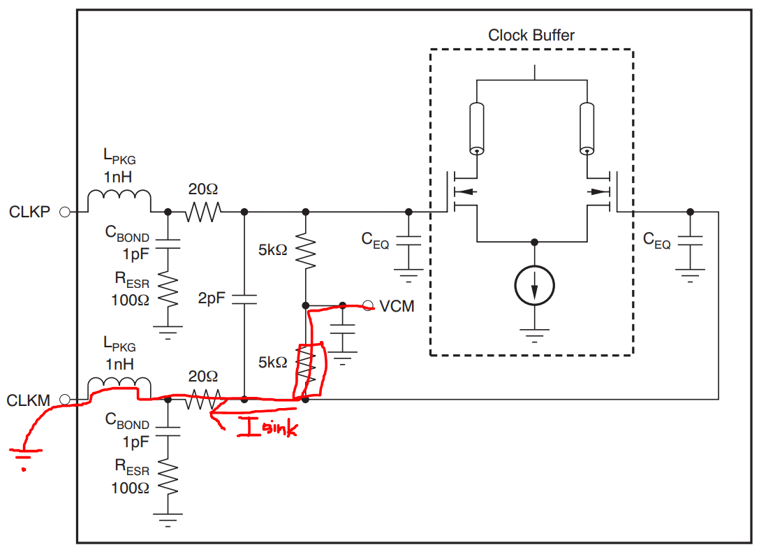
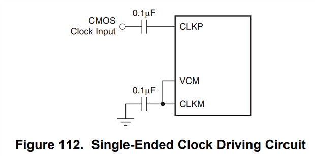
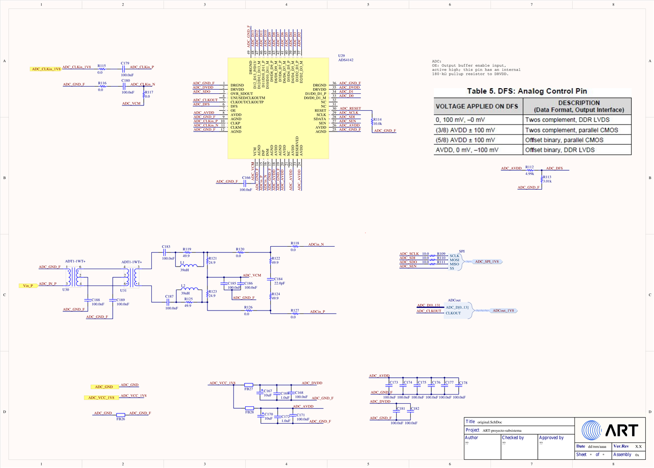
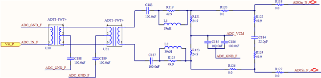
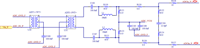
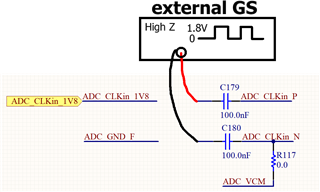
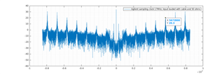
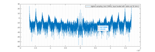
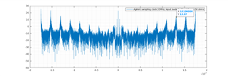
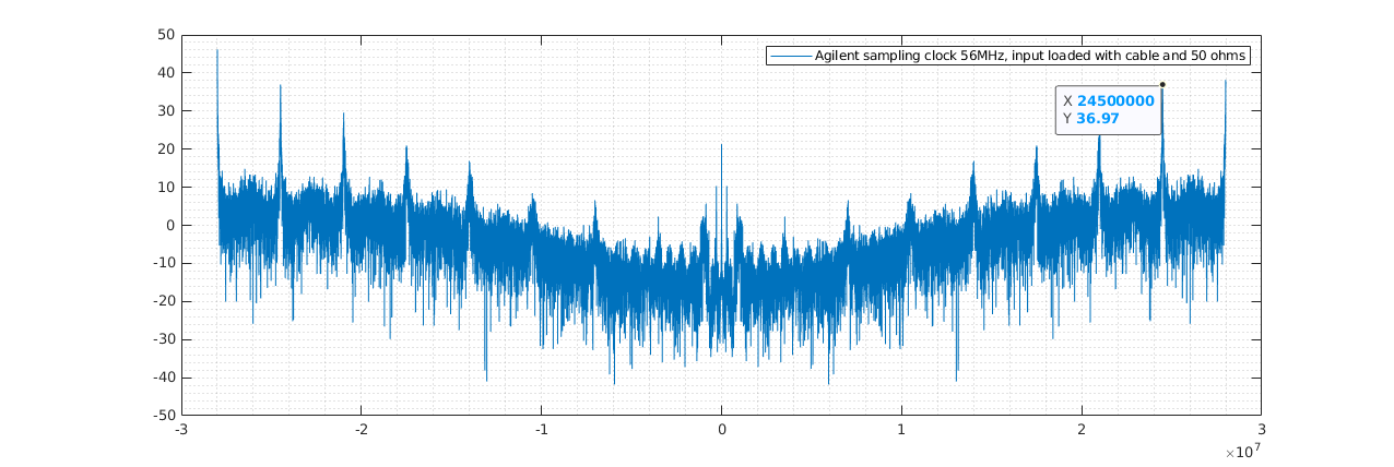
Hi, I'm trying to understand the circuit around Clk input. I see it allows for differential signals between CLKN and CLKP, and the circuit for a differential sinewave clock simply inputs into these pins. However, the CMOS example, instead of connecting CLKN to GND as I would expect, is connecting this pin back to the Vocm signal.

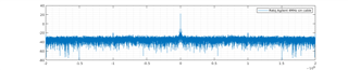
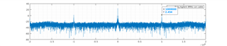
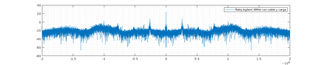
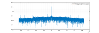
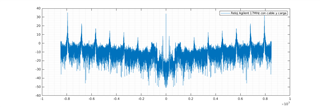
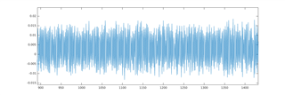
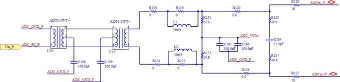
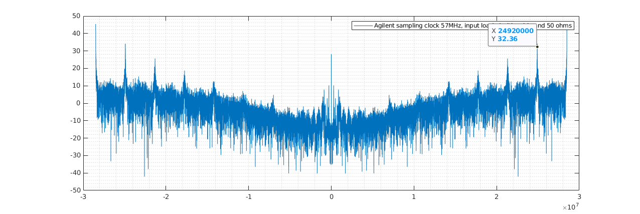
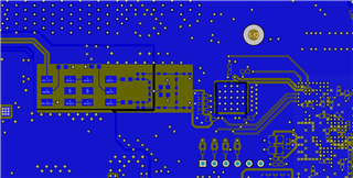
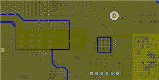
I have implemented my own board using this as a reference, as well as the input circuit based on two transformers. Measuring with an oscilloscope, I am seeing a very high noise appearing at Vin_p and Vin_n, and it looks like clock phase noise is being transferred to the input via Vocm signal.

I am not entirely sure if my noise is coming from the clock, but still I don't fully understand the clock input circuit, so I would like some insight on this. Could I just connect my 1.8V cmos clock to CLKP and CLKN directly to GND?

  • Hi Alvaro,

    The CLK P/M inputs are both internally referencing the VCM voltage through 5k resistors. If you connect the CLKM directly to GND, VCM will act as a current source. ( 5k resistance from VCM (0.95V) to GND -> 0.95V/5k = 190uA current source.) This will not improve the performance. I'd look elsewhere for this coupling issue.

    Is your single-ended CMOS clock source AC coupled (swinging between -0.9V through +0.9V)? or is this DC coupled (0V to 1.8V)? Is the CLKM and VCM connected to GND through a 0.1uF decoupling capacitor as shown in figure 112 above? Is it possible for you to measure the frequency using your oscilloscope? Something else to try would be to slow down the clock frequency to 10x slower just to check if the coupled tone is also reduced by a factor of 10x. Alternatively, you may connect a second channel (from the oscilloscope) to the clock input and check if the high frequency component on the input matches the clock. Is the input circuit you are referring to our EVM schematics? These are all just ideas to think about over the weekend. We can investigate this further early next week! 

    Regards, Chase

  • Hi Chase,

    Thanks for the explanation regarding CLKP/CLKM and VCM. Our circuit is as Figure 112 and it's swinging between 0V and 1.8V.

    We've tried different clock generators and we're always getting the same kind of high and unexpected noise. The board is designed to use a clock generated by an FPGA and we thought this could be the cause of our problems, but we've also tried with laboratory grade equipment as clock source and the level of noise hasn't changed much.

    We have, however, discovered something pretty unsettling for which we haven't found any explanation yet. The good news is we have some data captures so maybe you can help us diagnose this, which seems to be related with the analog frontend before the ADC itself. Our original circuit resembles very much that of Figure 108 of the datasheet, and is similar too to the one in the evaluation board. By removing/replacing by 0 ohm resistors some components, the current status of the board is equal to that of Figure 109.

    And the strange thing that we've discovered is that the board by itself seems to be capturing a noise floor that is in correspondence with the SNR of the ADC, but the result changes when a cable is connected to the input.

    All captures are made with 16384 samples at 4MHz scaled from ADC binary values to voltage, and plotted as 20*log10(abs(fftshift(fft(X)))).

    Open input:

    Open cable (1m length) connected at input:

    The almost catastrophic 1m length cable terminated with a 50 ohms load:

    Using 17MHz, which is our intended sampling frequency we have this case for an open input:

    And this is the completely catastrophic 1m length cable terminated with a 50 ohms load sampling at 17MHz:

    Which is so ridiculous that even in the time domain you can see something is wrong there:

    So, what we thought was due to a noisy clock is instead a very strange load effect that is happening around the input circuitry.

    Somehow, choosing a longer or shorter cable doesn't affect the results, except for the fact that it seems to require a cable long enough for the noise to appear (open 20cm cable won't cause the noise that an open 1m cable produces), but the frequency of the harmonics does not change depending on the length of the cable.

    So... we're quite lost, I don't even understand where the energy may be coming from to cause these oscillations and noise, since the input stage is completely passive. Any insight you can provide will be extremely useful.

    Thanks!

  • Hi Alvaro,

    In order to troubleshoot this issue, please share the schematic or block diagram of where the cable connects to your board and the input circuitry involved before this connects to the ADC's analog inputs.

    Regards,

    Rob

  • Sure, here it goes. Thanks.

    This is our original schematic

    Original schematic

    And these are the different tests we've tried around. The only thing that has managed to reduce a bit the noise was replacing R119 and R125 with 0 ohms resistors, thus shorting the inductors. All current tests and previous figures and captures are being made as in the circuit of Test5 with external clock. Before replacing R119 and R125, the results were even worse.

    Original analog frontend:

    Tests:

    Test1:

    Test2:

    Test3:

    Test4:

    Test5:

    Tests with external clock generator:

  • I am uploading several captures. All of them have been made with a 1m cable connected to the input connector and ended with a 50 ohm load. In both cases the oscillator is an external Agilent 33250A signal generator, set to High Impedance, square signal from 0V to 1.8V.

    The first one is that of a capture made with a 17MHz sampling clock. The second one is  made with a 34MHz sampling clock.

    Whatever this noise comes from, I would have expected to see the peaks at the same place. I understand that sampling at 17MHz vs doing it at 34MHz could be causing heavily aliasing, so for that reason I made an additional sampling at 35MHz.

    The position of the oscillations did change also, so I am thinking that this is either a very high frequency oscillation that is being shown due to aliasing on my lower frequencies (and thus the reason why it changes positions between sampling at 34MHz vs 35MHz) or there is something seriously wrong with my clock circuit (which I would discard as the circuit is very easy and you just explained this to me) or the ADC is somehow broken.

    To test this, I've made another two captures at 55MHz and 56MHz. The peaks are also changing positions, so this very high frequency oscillation should be even higher above.

  • Hi Alvaro,

    The Agilent 33250A would not be a suitable source for a clock for this type of ADC. I would recommend a low phase noise oscillator or signal generator with a filter in series with the output of whichever is handy.

    Lets start there first.

    Second, I would also remove R117 on the negative side of the clock input. The common mode voltage will be self biased. Please just put Cx to ground directly on your board.

    Try these two things first and let me know if the results have improved.

    If you need further guidance on testing converters.

    Please Google AN-835. This will give you a good sense on the types of clock and analog input signal generators needed, as well as filters, oscillators, etc.

    www.analog.com/.../an-835.pdf

    Regards,

    Rob

  • Hi Rob

    I've removed R117 so there's no connection now between Vcm and CLKM (although this contradicts the datasheet: Figure 112 requires it and that's why we put that connection there but since we were suspicious of it we placed a 0 ohm resistor on its way). However, there's no visible change.

    We are trying to rig something to connect a good oscillator/crystal to the ADC, but even though the 33250A may not be a perfect clock for the application, I can't believe it can be responsible of oscillations that are up to 60dB above the ADC noise as per my figures above...

    Thanks!

  • Hi Alvaro,

    Yes, signal source being used would be responsible for this poor performance for sure. The 33250A is a lab bench, 8bit DAC with poor phase noise.....if that. You are essentially testing your test equipment Slight smile since your ADC is a 14B with an SNR of 70dB or more. Your 33250A does not have that kind of dynamic range unfortunately. AN-835 should describe that pretty well.

    Please find a better clock source and send us a new FFT of the noise floor with no analog input connected.

    On the negative input of the clock, please ground C180 locally and reinstall R117. My bad on that one. Not typical for most single ended input configurations. 

    Regards,

    Rob

  • Well, when you put it like that it really seems like a poor choice of a clock Slight smile I am currently somewhat limited on lab equipment, but I'll sure find a way to feed this a better clock on Monday and send you new captures.

    Still, I can understand that a bad clock will sample a signal with lots of jitter and suffer greatly in its SNR. But right now I'm not sampling a signal but a long cable and maybe a load. I really can't understand the results, thermal noise shouldn't care about being sampled jitterly... I'm really really confused!

    I'll get back to you once I am able to use a good enough clock. Thank you!

  • Hi Alvaro,

    I will try to set this up in the lab myself on Tuesday and show you the difference between a FFT with a function generator as clock and a low noise sig generator.

    Stay tuned.

    Regards,

    Rob

  • Hi Rob,

    I managed to rig a setup using some boards I had lying around. The base clock is a ccso-914x-1000 that is feeding an AD9910. Sadly, I can't use the real DDS output but instead I need to use the DROVER signal this chip provides. The way it works is that I generate a double sweep from one frequency to another, and back from the second to the first. CMOS signal DROVER generates a pulse when the sweep changes directions. This pulse is passed as clock to a T flip-flop, whose output generates a 16MHz 50% square signal that I am feeding the ADS4142. I know this setup is a bit strange, but the resulting signal has very low jitter. This signal we use typically on our systems as trigger

    I am attaching the two usual captures: one without anything connected at the input and another one with a 50 ohm load. I can't notice any qualitative differences, and the "all goes to hell when loaded" phenomenon seems to be as bad as before.

    I'll try to simplify my setup because it's admittedly strange, but that's for now what I can provide. In any case, truly, I understand that my noise floor may be higher than expected due to my sampling clock. But what I can't really understand at all is what is happening when I add a long enough cable or a 50 ohm load. That shouldn't happen at all, regardless of the clock, I can't really think what could cause such a thing. I'm really at my wits end.

    Thanks!

  • Hi Alvaro,

    Just to be clear the FFT plot on the left is only a noise floor? and the FFT plot on the right, is when you connect a 50ohm load and/or cable to the analog input, U30/transformer for example?

    On the analog inputs, can you try measuring the common mode DC voltage at R120 and R126 for example? It should be about 0.95V.

    Next, I would try using an oscope at both those two resistors as well to make sure you are getting what you expect.

    Lastly, how are you capturing the data? With our data capture board or something else? I imagine you are using your own. It might be good to check that you are pullin gin the digital data correctly by turning on the ramp pattern in the ADC. This will allow you to test out the digital format and connections.

    Try those tests next and keep me posted.

    Thx,

    Rob

  • Just to be clear the FFT plot on the left is only a noise floor? and the FFT plot on the right, is when you connect a 50ohm load and/or cable to the analog input, U30/transformer for example?

    That is correct. When, instead of a load I connect a sine signal, I can see the tone at the right place, but with all that noise also.

    On the analog inputs, can you try measuring the common mode DC voltage at R120 and R126 for example? It should be about 0.95V.

    Next, I would try using an oscope at both those two resistors as well to make sure you are getting what you expect.

    Will do as soon as Ican and report back to you.

    Lastly, how are you capturing the data? With our data capture board or something else? I imagine you are using your own. It might be good to check that you are pullin gin the digital data correctly by turning on the ramp pattern in the ADC. This will allow you to test out the digital format and connections

    Yes, it's our custom zynqmp based board. First thing I did was indeed the ramp test and also the alternating pattern. Both of them were successful and we did not catch a single bit error with a 17MHz sampling clock.

    I'll post back again when I have those measurements you asked me for 

    Thanks!

  • Hi Avaro,

    Thanks for the update. Keep me posted on what you find out.

    Would it be possible to send over your entire schematic file for me to review?

    Thx,

    Rob

  • Hi again!

    On the analog inputs, can you try measuring the common mode DC voltage at R120 and R126 for example? It should be about 0.95V.

    We've measured at both points with Fluke 115 multimeter and it did measure 0.954V.

    Next, I would try using an oscope at both those two resistors as well to make sure you are getting what you expect.

    Our oscilloscope is also quite limited as it's a USB unit with limited bandwidth, but I think the following measurements should be representative, as its sampling frequency is 16MHz which is the 17MHz clock we feed the ADS4142.

    The results are extremely surprising, because there doesn't seem to be a significant difference between measuring at both points when there is or there isn't a loaded cabled connected to the input. So... somehow the ADC is capturing something that isn't there? I'm quite more baffled than before capturing this. These are captures on R120, those at R126 are more or less the same.

    Tomorrow I will be able to measure the difference between both chains, so I can see exactly what it is that is input to the ADC via the differential pads.

  • Hi Rob

    I will have to ask my boss about that, I cannot make it public but I believe I will be authorized to send it to you privately if you provide me a means of contacting you directly. If we discover what it is that is wrong, I won't mind at all publishing here our discoveries for other people to learn about it.

    Thanks again

  • Okay Alvaro, 
    I will send you an email directly.

    So you can send this to me.

    Regards,

    Rob

  • Taking this E2E post offline to solve.

  • Hi

    Just so this thread doesn't stays unsolved and in case it helps someone. Rob was very kind and after sharing the schematics with him we determined that we had some division on the grounds that should probably be rethought, but the specific cause of this very strange issue was a mistake that somehow escaped our reviewing process.

    Due to some mistake, this plane isn't directly above the analog frontend that goes before the ADC, and as it can be seen on the left image, the plane cuts in the middle of the circuit, making the differential signals that go into ADCin+ and ADCin- suffer the consequences.

    We were able to replace this chunk of the circuit with a small testing board with the same circuit but properly grounded and the issues disappeared, so clearly this defective routing was at fault.

    So, the lesson of this is: think well your grounds divisions if you need them, and learn how to review your own circuits Slight smile We would have saved a lot of trouble and time if we had been able to catch this blatant error before manufacturing, so we'll have to review our reviewing procedure. Let's hope the review of the reviewing is best reviewed than the circuit reviewing itself Stuck out tongue closed eyes.

    Special thanks again to Rob!