This thread has been locked.

If you have a related question, please click the "Ask a related question" button in the top right corner. The newly created question will be automatically linked to this question.

ADS8668: AGND/DGND/GND

Part Number: ADS8668
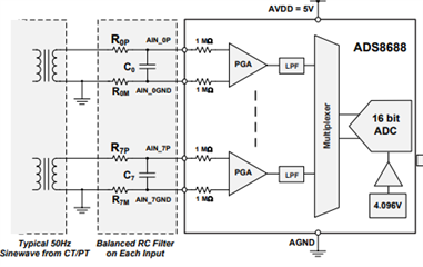
Other Parts Discussed in Thread: ADS8688

Hello,

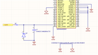
We are using COTS industrial System on module and it has ADS8668 on that board. However, we can't get internal schematics for it. 

On their pinout I can see Analog IN and Analog GND. When looking with multimeter, the Analog GND has continuity with overall GND in the system.

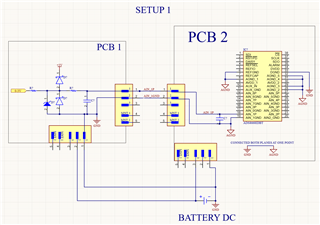
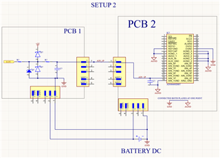
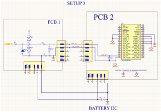
We want to use ADC inputs to measure some voltages in the system (such as battery, capacitor voltages). It doesn't need to be extremely precise. 

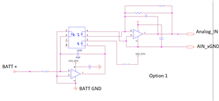
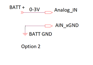
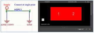
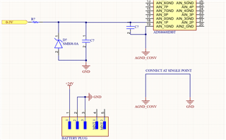
The Analog IN is coming from our PCB, and we don't have isolation between AGND and DGND. We have Battery GND connecting overall system GND. What harm it would be connecting the Batt + straight to Analog IN and connecting Batt GND to Analog GND (as I mentioned above, when checking with multimeter Analog GND already has continuity with overall system GND which is connected to Battery GND)? 

Thanks 

  • Hi Sarunas,

    The AGND of ADS8668 should not be isolated from the DGND of ADS8668, actually a solid ground plane is recommended for the AGND and DGND of ADS8668. I do not know if your Analog IN is actually connected to the positive input of the ADS8668 (AIN_xP). If yes, you can connect your Batt+ to Analog IN. If the system GND is connected the AGND&DGND of the ADC, you can connect your Battery GND to the system GND. Make sure the AIN_xGND is connected to the AGND&DGND of the ADS8668 as well.

    Let me know if you have any questions about ADS8668, thanks.

    Best regards,

    Dale

  • Thanks for a reply. that is really helpful. 

    The system is powered by Battery. All grounds are referenced to BATT GND. So in that case, I can also see on SOM that AIN_xGND is connected to DGND and connected to BATT GND. Having said that, there is no need of optoisolators then if the wires are very short. Or they still need to be isolated? Would Option 2 would bring some problems? THanks 

  • Hi Sarunas,

    I do not see any issue to use the option 2.

    If an isolation (optoisolator) is expected by you and you are planning to use the option 1, you will have to use a separate ground for BATT GND and the ADC ground. 

    Regards,

    Dale

  • Thank you that is really helpful from You. Does AIN-xGND needs to have  a capacitor connected between Analog IN for decoupling?

  • If option 1 is used, there won’t be any benefit or any isolation if the AGND is connected to DGND which is connected to whole system BATT GND. Correct me if om wrong at this point? 

  • Hi Sarunas,

    This ADC has an integrated analog front-end with 1Mohm input impedance on each channel, so it does not require an amplifier to drive. A RC filer is usually placed for filtering between the sensor/source and the ADC input, check the figure 124 in the datasheet and also the schematic in the ADS8688EVM user guide.

    For your option 1, 

    • If the BATT GND is shorted to the AGND and DGND, I do not see any benefit to use an optocoupler just for signal. If you want to protect the ADC input, a protection circuity can be designed.
    • If an optocoupler is used for signal and also the BATT GND is isolated with AGND and DGND, this is helpful to completely isolate them. However, notice that this ADC can not sample a signal with high common-voltage.

    Regards,

    Dale

  • Thank You so much. I've looked at the ADS8688 design on a board. AGND is connected to whole system GND at one point. So I'm assuming still optoisolation is not needed if protection circuit is present?

    Thanks 

  • Hi Sarunas,

    I'm not sure what protection you want. If you are talking about electrical overstress (EOS) protection. Please see more information at Precision Labs ADC - EOS series.

    Thanks&regards,

    Dale

  • Hi Dale,

    Many thanks for your answers and input. Last request: Would you be able to take a look at this ground concept and see if the grounding structure seems correct? The AGND is connected to system BATT GND at one point. Input to ADC is coming to AIN_1P from other board through the connector and short wire .AIN_GND is connected straight to AGND ground plane through the via. Decoupling capacitor between AIN and AIN_GND is attached too. 


  • Hi Sarunas,

    I saw the R? resistor is used prior to the TVS diode, are the resistor and TVS diode used for over voltage protection? Regarding the ground, I do not see a reason why the AGND_CONV is connected to the GND through a single point.

    Thanks&regards,

    Dale

  • Hi Dale,

    Thanks for a reply! Yes R/TVS is for overvoltage. Don't look at the values, they are just for showing purpose. The question I mean, if the signal is coming to the AIN, and AGND and DGND is connected to one plane at one point, does AIN_xGND can be connected to system GND plane straight through via, or it has to be connected to AGND (even though AGND and GND/DGND are still connected together). See a photo as reference if it does make sense? Many thanks.

  • Hi Sarunas,

    The AIN_xGND should have a same voltage potential as the AGND (<100mV), I do not know how far your via is designed from the AIN_xGND and it may be connected through a long trace. As recommended in previous post, a solid ground plane especially for AIN_xGND, AGND and DGND is suggested, then the ground plane can be shorted to your system GND.

    Regards,

    Dale

  • Hi Dale, thanks for your reply. Sadly, I can't see how ADS8668 was designed on that off the shelf computer board. But I know the AGND/DGND/AIN_xGND are all connected. All PCB's are powered by one battery and shares battery GND. MY only question though they giving a connector output with AIN_xP and AIN_xGND contacts available. So to avoid GND loops would you recommend SETUP 1 or SETUP 2 or SETUP 2?  Don't look at the component values as they just for demonstration. Thanks for your golden patience. 

  • Hi Sarunas,

    Thanks for your clarification. Unfortunately, I would not recommend anyone of them. First, setup 2 is not recommended because of a longer ground loop between pcb 1 and pcb 2. Second, the only difference between setup 1 and 3 is the resistor on the GND on pcb 1. The balanced RC filter should be placed close to the ADC's input, below is an example from the ADS8688 datasheet.

    Regards,

    Dale

  • Thanks Dale for your patient. I agree with longer current loop on SOLUTION 2. What would you recommend if isolation is not needed? Or would you recommend using an isolator? The ADC will be monitoring some capacitor voltages and power supply rail. Where that AIN_xGND should be connected then ? Would you still route that cable to PCB1 and connect to PCB GND as close as possible? And lets consider that balanced RC filter is present as close to the input.What would you recommend? Thanks. 

  • Hi Sarunas,

    If the pcb board 1 is needed, use setup 3 but move the balanced-input RC filter to the pcb board 2 and place them close to the ADC's input.

    Regards,

    Dale

  • Dale, you are amazing helping with this. Last question I guess. If the cable between the boards is around ~40cm and the precision is not really needed. I'm assuming the FILTER marked in red rectangle is not needed? Also, would you leave TVS with clamping diodes? See photo attached 

  • By the way, would you recommend buffering the ADC IN because there is a cable coming from other board? If yes, any IC to recommend from Texas Instruments? 

  • Hi Sarunas,

    Sorry for the late response because of the weekend. ADS8688 has integrated an analog front-end (AFE) including a ADC driver on each channel, so no op-amp is needed to drive the ADC. Also, a 15kHz BW LPF is included in the AFE on each channel, so any external filter >15kHz BW will not help to filter noise, however the series resistor will help to limit input current, so usually a LPF is suggested. Using diode(TVS or Schottky) depends on whether there is overstress or transient signal in your design or not. If there is no such situation, no extra protection is needed.

    Regards,

    Dale

  • Hi Dale,

    many thanks for this. I will be using the OPTION 3 between 2 PCB's and the AIN_xGND wire will be connected to another PCB GND as close to measurement point. Would you then recommend adding a LPF with 15kHZ cutoff frequency on other PCB? 

    I think that was a last question! Your help is much appreciated. 

  • Hi Sarunas,

    It's not needed for ADS8688 design, however you can if you really want.

    Regards,

    Dale

  • Thanks Dale. And if I would include the LPF on PCB 2, it has to have 15kHz cutoff frequency? I just received schematics from SOM board of ADS side. It includes balanced filter so I guess no filtering is needed on PCB2

  • Hi Sarunas,

    I do not understand your question. As I said, ADS8688 has integrated a 15kHz LPF on each channel. You can use a lower BW RC filter on ADC input to filter more noise, however, the larger value series resister can lead  to a gain error comparing with the 1Mohm input resistance. You can use a higher BW RC filter too which will not help to filter noise too too much because of ADC's internal LPF.

    Regards,

    Dale