


Part Number: ADC32RF42EVM
Other Parts Discussed in Thread: ADC32RF42
Hello, I use your ADCRF42 chip to support my own customized ZYNQ development board for high-speed data collection. At present, the problem is that the link cannot be established, the CGS state cannot be entered, and the BC code cannot be received on the FPGA end. I checked a lot of posts and still couldn't find the problem. Please help me!
The clock configuration is as follows:
ADC:Fs=750MHz SYSREF=1.171875MHz
FPGA:CORE CLK=187.5MHz reference clk=187.5MHz SYSREF=1.171875MHz
The clock's frequency and amplitude are generally fine
The AD configuration is as follows:
I used the GUI example Configuration file BYPASS ADC32RF42_4222 mode
The following two places have been modified
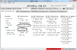
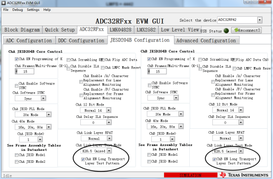
Can the AD terminal enter the test mode and send K codes in this configuration mode?
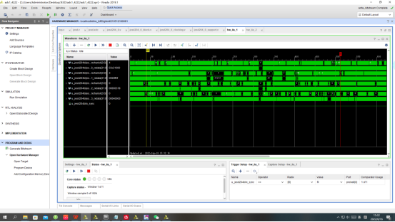
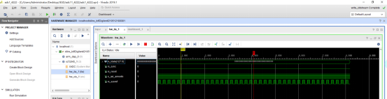
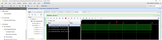
Register 038= 0x0001_0000
Register 03C= 0x0000_0000
Register 004= 0x0001_0000
I check with the following method:
- I checked the configurations of AD and FPGA
- I checked the clock
- I checked the three reset signals and the QPLL LOCK signal
- Constraints are checked
No problem. I was really confused for a long time. I would appreciate it if you could give me some advice
Best regards
Kailyn
