This thread has been locked.

If you have a related question, please click the "Ask a related question" button in the top right corner. The newly created question will be automatically linked to this question.

DAC8820: Settling time clarification

Part Number: DAC8820
Other Parts Discussed in Thread: OPA2277, OPA277

Hi All,

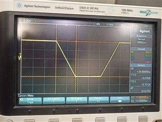
 I am using DAC8820ICDBR in Bipolar mode of operation(-10V to +10V) with -10V as Vref in my design. For DAC8820ICDBR, settling time for switching from -10V to +10V is 28us. But the same when measured in DAC8820EVM showed around 8us. Whereas in Datasheet, settling time is mentioned as 0.5us.  Please find below the circuit connections used in my design.

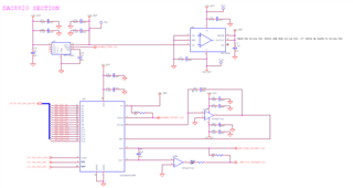
We have given similar connections as in DAC8820EVM. Can anybody pls explain why is the settling time changing even after retaining the same circuit?

  • Hello,

    Are you measuring the settling time at the output of the amplifier? The settling time of unbuffered DACs is limited by the external output buffer chosen. The 0.5us spec from the datasheet is only for the performance of the DAC output. 

    Best,

    Katlynne Jones

  • Hi Katlynne,

    The settling time is measured after OPA2277 in both Eval board and Custom board. 

    In Eval board, it settles in 8us.

    But in Custom board, it is taking 28us. Kindly help me why it is behaving differently for the same schematic circuit.

    Also in datasheet  it is mentioned that voltage can be measured only after OPA2277 only. Before that it is current output only.

    Regards,

    K.A.Rajeshwar.

  • Hi K.A.

    Lots of factors can effect settling time for an unbuffered DAC and output amplifier.  Note the the RFB pin has about 12kΩ of resistance, so any cap load on that node is essentially creating an RC filter on the transimpedance amplifier.  

    There are a few measurements that I recommend you do:

    1. Measure the REF pin - does updating the DAC result in the reference voltage changing significantly?

    2. Make sure when using your scope that the y-axis or volts/division is sufficiently large enough that the ±10V step can be captured without clipping.  When the output clips, you might be seeing some kind of overdrive recovery rather than settling time.

    3. Is your custom board a single PCB? are the traces between the DAC and the output buffer short and direct?

    Thanks,

    Paul

  • Hi Paul,

    Kindly find the observations below. 

    From schematic you can see that there is no capacitor placed in the RFB pin.

    1. We have measured the REF pin during DAC update and the voltage changes between +/-30uV from -10V ref input.

    2. I have attached the DAC Output waveform captured in our board.

    3. Yes, our custom board is Single PCB. The traces between DAC and Output buffer short directly.

    Regards,

    K.A.Rajeshwar.

  • Hi K.A., 

    Is C85 installed?

    Best,

    Katlynne Jones 

  • Hi Katlynne,

    I have tested the settling time with C85 placed and removed. But no difference found.

    Regards,

    K.A. Rajeshwar.

  • Hi K.A.,

    The scope shot you have shared is consistent with the slew rate of the OPA277. if you check the datasheet then you will see that the slew rate is 0.8V/us. This will come out to ~25us for the 20V step (-10V to +10V).

    Did you test with the same 20V step when you measured the output on the EVM?

    Best,

    Katlynne