This thread has been locked.

If you have a related question, please click the "Ask a related question" button in the top right corner. The newly created question will be automatically linked to this question.

ADS8688A: accurate leakage current values?

Part Number: ADS8688A

Team,
Can you please help with the below?

I am looking for accurate leakage current values. On the datasheet, section 7.5, there is the Input leakage current formula. Considering the input range as 1.25 × VREF, the formula is:

My questions about that would be:

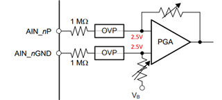
  1. is the voltage between the AIN_nP pin and GND or between AIN_nP pin and RTN?
  2. What is the current flowing through the RTN pin to GND? Does it follow the same formula?
  3. Maybe you could clarify the way the input supply is connected to come to that formula (i.e. supply and RTN connected to GND)
  4. Is the “2.5” number always constant and accurate? Would you have a tolerance value for that? Does the value change with temperature drift?
  5. Is Rin always the input impedance Zi (from 0.85 MΩ to 1.15 MΩ)? If I have resistors in series with the input, should I consider it here?
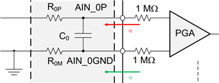
  6. If you have any equivalent circuit for me to base on and maybe include more details for the formula, that would be great. For instance, something like the picture below, but more detailed (resistor values, internal bias voltages, PGA gains, etc

Thanks in advance,

A

  • Hi Anber,

    1. I'm not sure what RTN pin you mentioned is, however the Vin is the voltage between the AIN_xP and AIN_xGND which is normally connected to the AGND.

    4. The 2.5V is a typical value. We do not have more data about it including accuracy and drift, however it will not have any impact to convert your analog signal which is applied to the AIN_xP pin. This is a internal bias voltage. for PGA.

    5. Yes, the impedance is guaranteed in the specified range. If your series resistor is too large, it will lead to a gain error because it forms a resistor divider with Rin. Also, it will affect THD performance.

    6. The details about the internal circuity can not be shared. Can you clarify what your concern is in your design?

    Regards,

    Dale

  • Hi Dale,

    Thank you for your previous answers.


    For item 5 and 6, I would like to clarify the implementation of a possible RC filter, as also suggested on some application articles. If R0 is too large, it will form the resistor divider, as you mentioned. The leakage formula is not clear about what happens the AIN_xGND. If AIN_xGND is connected to GND through a resistor (ignoring C0 impedance and leakage), some voltage can be seen on AIN_xGND (respective to GND) due to the current I2. I have measured around 2.5uA between AIN_xGND and GND (with amperometer, no series resistor).  
    That is the reason why I would like to have a brief understanding of the internal circuitry (in a simple way) in order to be able to simulate/calculate the behaviour of AIN_xGND when there is a series resistance. For instance, I would maybe model it with a 1M resistor in series with a 2.5V rail, resulting on the same formula for the AIN_nP pin and AIN_nGND. Sorry for going so deep into that topic, but it would be good to evaluate how the current flowing through AIN_nGND can affect voltage readings.  If you have any information about that topic, please let me know. Thank you in advance.


  • Hi Anber,

    The reason we suggest to use a balanced-input RC filter (R0P and R0M resistors) is, it can cancel the offset which is caused by the leakage current is flowing through the R0P resistor in the unbalanced RC filter (only R0P resistor). In other words, the error caused by the leakage current through the R0P resistor will be cancelled by the error caused by the leakage current through the R0M resistor when the balanced-input RC filter is used. Therefore, you do not need to worry  too much about the leakage current if you are using a balanced-input RC filter on the ADC input.

    Regards,

    Dale