This thread has been locked.

If you have a related question, please click the "Ask a related question" button in the top right corner. The newly created question will be automatically linked to this question.

DAC7750: DAC7750 easy to damage issue

Part Number: DAC7750
Other Parts Discussed in Thread: DAC8750, DAC8775, DAC8771

Case one, DAC7750 load 0~1K ohms change, with a multimeter current gear parallel at both ends of the load, DAC7750 is easy to  be damaged;

Case two: The power supply has the function of hot swap, and DAC7750 in the charged board card has been damaged in the process of inserting tightly;

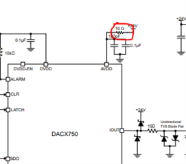
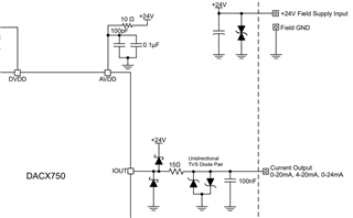
The principle diagram is as follows, whether the design problem causes easy damage, and whether the CIRCUIT CAP1&CAP2 is related to the slew rate. At present, this part is not designed.

DAC7750.docx

  • Hi,

    Just to clarify, Case One and Case Two are theoretical situations that have not yet been implemented?

    Thank you,
    Lucas

  • Dear Lucas:

    I do not understand what you mean, after case 1 & case 2 DAC7750 ‘s’ pin  impedance to ground is abnormal, so need you help me judge and analysis ;whether the schematic is ok  and how to check ? why is only the dac7750 be damaged ?  please kindly help me check whether it is referred  to CAP1 & CAP2 design ? 

  • Cooper,

    I have heard of cases where the supply ramps quickly (on the order of 1V/ns) which can trigger damage in the device. This was recently put into the datasheet in the Power Supply Recommendations on page 40. If the supply is hot-swapped (where the supply is placed in parallel with a low ESR bulk capacitance, you my see this type of fast transient. Similarly I would guess that in some cases IOUT has some inductance where the current may cause some transient to damage the device when there is some instantaneous change in load, like a output from a resistive load to a short, or from a resistive load to an open. I don't think that the CAP1 and CAP2 values would make any difference in this effect.

    In either case, I think that the damage would likely be some sort of low resistive path from IOUT to GND, where the damage occurs at an ESD pin. 

    What we've recommended is that you have some amount of series resistance from the supply to AVDD. In this case you have F_24V_AO, and you could use a 10Ω resistor in series to AVDD. In the datasheet we show this in page 37 of the typical application. It is on the upper right hand corner of the device.

    The series resistance serves two purposes. First, this causes a slower ramp of the power supply seen at AVDD as an RC filter. Second, this series resistance reduces any possible current that may be sunk into AVDD during fast transient event.

    Let me know if you have any further questions.

    Joseph Wu

  • Thank your quick reply, i will try it.

  • I want to ask a question, AVDD has a 0.1uf and 100pf capacitor in recommended circuit, then in my circuit i use 1uf and 0.1uf, then i must change the capacitor value as the recommended circuit?

  • Hi,

    Generally, I don't think that should be an issue. I've never heard of any problems with a larger capacitance.

    Joseph Wu

  • Joseph:

           I have tested three chips, they are still damaged

           The chip is fragile. I need furthe support. DAC7750_load_change_test.docx

  • Hi Joseph:

    customer has tested as below , but  it is still damaged ,whether there are further optimization methods to deal with ? 

  • Hi,

    Do you know what pin might be damaged? Is there extra current coming from the BOOST pin or is there extra current coming from IOUT?

    Generally, we use two different methods of protecting pins from damage. First, we often use diodes so that if there are over-voltage events, the pins get latched pins to the supplies. Excess current is shunted back to the supplies or ground. Second, series resistance is used to make sure that the current pulled out of the pin is limited. For the DAC8750, this is what we show in the datasheet for the output protection.

    In this case, the BOOST pin is not used. The low-voltage Schottky diodes limit the over-voltage at the pin to prevent the internal diodes from forward biasing. In the figure, the pin is directly protected. For the BOOST pin, you'd want something similar in protecting the pin from the over-voltage event. In your test, I think there might be an over-voltage event that is caused by inductance in the line when the current is switched in and out of the load and ammeter.

    In the schematic, The protection is far away from the pins. I would start with some diodes that strap IOUT to the supplies and strap BOOST to the supplies. Again, I'm not sure of the damage mechanism, so both may not be necessary. You would choose some low-voltage Schottky diodes reverse biased to supply and ground, similar to the datasheet.

    I'll be out of the office for Thursday and Friday, so responses back to this post may be slow.


    Joseph Wu

  • PIN19_IOUT is damaged,After the IC is damaged , PIN20_BOOST and PIN19_IOUT has only 77ohm resistor. Otherwise, the normal PIN20 and PIN19 has MOHM resistor.  So internal T2  in IC has been damaged and can not be adjusted according to outer load. AVDD directly output current from BOOST, T2 just like a low-ohm resistor.

    Because I worried about thermal problem, so I select outside bjt scheme.

    I have test this fuction through add diodes @ IOUT_PIN, it also failed.

    I oberved signal @IOUT_PIN when the IC is damaged, I didnot find overshoot or undershoot voltage event.

  • Hi, Joe will be out for a few days, and will take a look at this on monday.

  • Hi  Joseph:

    as below my top customer feedback

    PIN19_IOUT is damaged,After the IC is damaged , PIN20_BOOST and PIN19_IOUT has only 77ohm resistor. Otherwise, the normal PIN20 and PIN19 has MOHM resistor.  So internal T2  in IC has been damaged and can not be adjusted according to outer load. AVDD directly output current from BOOST, T2 just like a low-ohm resistor.

    Because I worried about thermal problem, so I select outside bjt scheme.

    I have test this fuction through add diodes @ IOUT_PIN, it also failed.

    I oberved signal @IOUT_PIN when the IC is damaged, I didnot find overshoot or undershoot voltage event.

    so,  whether is there other methods to deal with the issue?   if could not avoid risk,  customer has to change other solution , could you help promote suitable DAC ?

  • Cooper,


    If IOUT is damaged, I think it is likely that it is damaged by some inductive kick that brought the IOUT pin briefly below ground. That is why I suggesed the diode protection.

    However, the diodes type is very important. It must be some low voltage Schottky diode so that the forward voltage is as low as possible. This should protect the IOUT pin. What model diode did they try in their application? Something like a generic BAV99 might have too high of a forward voltage. A BAT54 type diode has a fairly low forward voltage and a low leakage even with a high reverse voltage. Also, did they add the series resistance to the IOUT pin. In the datasheet and the EVMs, I think we add a series 15Ω resistor to IOUT.

    To make sure of their tests, were you able to get their schematic? It might be good to review it to see if there are any other recommendations.

    If they want to review other devices, the DAC8771 is another DAC that has a similar set of features. It has both current and voltage outputs and integrates a buck-boost converter for the supplies. It also comes in a four channel option called the DAC8775.


    Joseph Wu

  • Thanks Joseph:

    the schematic as attached , I will share the suggestion to customer and discus,please kindly help check the schematic again , many thanks

    4571.DAC7750.docx

  • Cooper, 

    I was hoping that there would be a schematic with the changes made to help protect the circuit. That would include the series 10Ω resistors and the location of the protection diodes. I'd also mention that in the circuits in the datasheet, we've had 15Ω series resistances to IOUT. In the boost transistor version, we don't show that, but it would probably be good to insert 15Ω resistors at IOUT and BOOST.

    Joseph Wu

  • Thanks for your reply.

    BAT54 has VRRM=30V.

    Here I want to use RB751S40.VRRM=40V, File: RB751S40 Schottky Barrier Diodes.pdf
    As your recommendation: I want to change as below doc.

    1、But your know add R190( or add more R191) will add PCB area and power consumption. Did  i only use R190.
    2、I also want to know whether the power of RB751S40 is suitable?

    APP_DAC7750_SCH_Improvement.docx

  • Hi,

    I would guess that that the RB751S40 would work ok, but the BAT54 does have a lower forward voltage which I think would be safer.

    In your tests did the BOOST pin also get damaged? It may be susceptible to damage similar to the IOUT pin. If the BOOST pin also was damaged, you may need a similar diode structure to protect the pin.

    For the board, I would certainly use the R190 to limit the current flowing from the supply. For the circuit, we've recommended 10Ω instead of the 20Ω shown in your circuit. That should at least reduce the power dissipated across the resistor. After that, I would insert some series resistance going to BOOST as you've shown in figure 2 and going to IOUT as you've shown in figure 3.

    One last thing is that I'm not sure if FB5 is necessary. Added inductance to the ground node seems a bit unusual to me. I would think that you would want the ability to shunt current to the ground node in an over- or under-voltage event without any restriction. You may want to remove that ferrite.


    Joseph Wu

  • Thank you for your reply

    1、It is not possible to confirm whether the BOOST pin is damaged. But it is confirmed that the impedance between BOOST and AVDD is correct, and the impedance between BOOST and IOUT becomes lower to 77ohm. IOUT and ground are high impedance.

    2、The change measure is

    1) Add a 10ohm (1210) resistor to the AVDD pin input to limit the current.

    2)  Add a 10ohm (1210) resistor to limit the current from the BOOST pin output to the external NPN.

    3) BAT54 protection is added to BOOST pin. 

    4) Add BAT54 protection to the IOUT pin, and then add a 1kohm (0805) base drive resistor.

    5) Remove the bead FB5 at the AO- connection.

  • Hi,

    The only small change I would make to this is to #2. Instead of a 10Ω resistor, I would use a 15Ω resistor to match the circuitry in the datasheet and EVM. I don't know of any specific reason for using 15Ω, but that was what was originally tested when the part was developed.

    If you've made the change to the schematic, can you show it? I just want to make sure that we have the same thing in mind.

    Joseph Wu

  • Hi,

    That looks like the protection that I would use. However, for the DN1 and DN2, I would still connect them to F_24V_AO instead of F_24V_AO1. If there is an over voltage event, I would want the diode to quickly shunt the over-voltage current directly to the supply (not through the 10Ω resistor).

    Once you make that change, I would test that circuit out with the original ammeter test.

    Joseph Wu

  • 7444.APP_DAC7750_SCH_Improvement_20220722.docx

    The newest sch.

    You say you will test this circuit, I think it is great.Since the principle has changed a lot now and there are too many devices added, I made secant lines on the pcb board and soldered the devices, resulting in the experimental results not being very good.

    So I want your result eagerly.

  • Hi,

    I'm sorry, but I think you misunderstood me. I meant that you should test the circuit. I don't have a board that has the BOOST circuit connected, so I don't have the primary connections to put this together. I had meant that I would test the board in that way if I were you.


    Joseph Wu

  • ok, I see.

    The test needs to be completed for a long time. 

    I have changed my sch and pcb drawing.  You can close this topic temporarily.  If I have latest news about this circuit, I will reply here.

  • Ok,

    I'll close this thread for now. Once you are able to test it, you can post to this thread. If you have problems posting, you can start another thread.

    Joseph Wu