This thread has been locked.

If you have a related question, please click the "Ask a related question" button in the top right corner. The newly created question will be automatically linked to this question.

ADS1232: What is the differential input impedance and single ended input impedance of the chip in the range of 0~60 ℃?

Part Number: ADS1232

The reason is that there are bugs in the company's existing modules

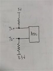
We need to modify the pull-up and pull-down resistance values of TC measurement disconnection detection circuit in the picture.

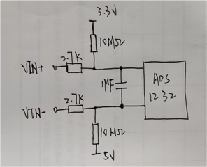
We plan to increase the existing 10MΩ to 50MΩ. If the input impedance is too small, the ADC input voltage will be too small when the sensor is not connected.

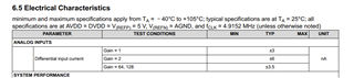
Only differential input impedance at 25 ℃ is seen in the manual.

  • Hi Rengui,

    The input impedance is relative to the dynamics of the sampling clock frequency.  A better indicator is the input currents.  The current is based on sampling and also leakage.  The sampling currents remain fairly flat over temperature, but the leakage increases as the temperature increases and starts to be more dominate at 85 deg C and above. 

    The input current specifications are shown as typical only and are not a guaranteed performance.  There are two basic forms of operation.  One is the bypassed amplifier inputs for gains of 1 and 2 where the input currents are higher.  The amplifier inputs are much lower current as the input follows an INA (op amp) input structure at gains of 64 and 128.  From the characterization data the absolute and differential currents for gains of 64 and 128 appear to be much better than given in the datasheet.  The current in the temperature of interest is below 1nA from the data.

    At a gain of 1 and 2 the input currents will be higher based on the input structure that bypasses the amplifier.  Based on the diagram provided the measurement will be using a gain of 1 or 2 as the input for TC+ is outside of the input range for gain of 64 or 128 ((AVDD - 1.5V) and the input is 5V).  From the data I see absolute input currents with outliers as much as 15nA with the majority between +/-6nA.  The differential current doesn't significantly change from the typical datasheet values over the desired operating temperature range.

    It is not clear as to what the original issue was with respect to the measurement, but using 50M resistors may be too large in gains of 1 or 2.  Experimentation would be required to validate the change.

    Best regards,

    Bob B

  • Hi Bib B,

    Thank you for your reply. 

    Is there any leakage current index of single terminal? That is, the leakage current of the pin to ground or power supply.

  • Hi Rengui,

    The values I mentioned in my last post as 'absolute current' would be the current that would include leakage for the pin alone.  As I stated above, device validation shows the leakage for the temperature range requested showing most devices in the +/- 6nA range with some outliers out to +/- 15nA for the gains of 1 and 2.  As the temperature increases beyond 50 degC there is increased leakage which is primarily through ESD structures and internal device switch nodes.

    As the only way to measure the current is through an individual analog pin there is no way of determining what is sampling bias currents alone and what is leakage to the supplies aside from knowing the CMOS and ESD structures from simulation.

    Best regards,

    Bob B

  • Hi Bib B,

    Sorry, after two communications, I still don't fully understand it. Let me describe the problem in detail.

    We use chips to collect thermocouples. The principle is shown in the figure below. Vin+ and vin- are input signals, with a range of -80mv~80mv, and the PGA configuration of ADC is 2. Two 10mMΩ are used for wire break detection. When the sensor fails, the input signal of ADC will certainly exceed 80mv. Because it is not considered that 5V will decrease with the increase of backplane module during use, the tested voltage range is 4.5v~5v. Due to the partial voltage of 2.7K Ω and 10MΩ, the acquisition error will be caused. When we test at room temperature, the 0.2V change of 5V will produce 80uv error. Because the hardware cannot be modified, we plan to reduce the error by modifying 10MΩ and 2.7K Ω. We want to adjust 10MΩ to 50MΩ

    I want to know about the input voltage of ADC caused by the input leakage current of ADC at 50MΩ? We hope that the input voltage is quite different from -80mv~80mv, and should be greater than 500mv as far as possible.

    Best regards

  • Hi Rengui,

    You might be looking at the cause of the error incorrectly.  Is the same varying supply (4.5~5V) used for AVDD and/or the reference voltage to the ADS1232?  If the AVDD or reference voltage varies you will see an error.

    The pullup and pulldown 10M resistors should actually be outside of the input filter path.  By changing the value of the resistor you are not really solving the problem only minimizing it by lowering the total current through the 2.7k resistors.

    As far as the current flow, if the thermocouple is open then there is no current flowing through the 2.7k resistors.  You should be able to measure the voltage with a voltmeter at each of the 10M resistors at the input to the ADC to verify.  What voltage is being measured at the inputs?

    If VIN+ and VIN- are shorted, then you will have current flowing through the 2.7k resistors which will add a voltage measurement error as the filter resistance is now a part of the measurement path.  It is this case where you will have both a voltage divider and a current divider.  I believe it is the current divider to which you are concerned.

    The 1.7V difference between 5V and 3.3V uses about 17nA of current in the path.  Assuming that only current is flowing through the path of the resistances there will still be abut 100uV of error from the filter resistors.  This is why you don't want the filter resistors in the current path for the measurement and the pullup and pulldown resistor should be outside of the filter.

    The current divider is created due to the sampling of the input (bias current of the measurement) and leakage current (which will dominate at higher temperatures).  The absolute current is the total current into the pin with respect to AGND.  The differential current is a dynamic current from the measurement.  It is dynamic due to the charge/discharge of the input sampling capacitance (when using gains of 1 or 2 as gains of 64 and 128 uses a higher impedance path of the INA).  There is also currents due to the input chopping to reduce input offset.

    As the input current is dynamic with respect to input voltage and sampling frequency, it is difficult without experimentation to know the specific outcome.  In other words you cannot determine the value of resistance for a DC current path in this case.  The impedance is determined based on an average for a specific input voltage.

    I don't believe there is a good way of determining an outcome by calculation.  I think this will require experimentation due to the circuit design.  I might be able to give more guidance if I know precisely the supply and reference voltage and the specific data relative to the testing.  It would also help to know which of the use cases (open or short) you are referring to that is showing the error.

    Best regards,

    Bob B