This thread has been locked.

If you have a related question, please click the "Ask a related question" button in the top right corner. The newly created question will be automatically linked to this question.

ADS124S06: False ADC readings with temperature increase

Part Number: ADS124S06

I am currently experiencing some issues with ADC ADS124S06IPBS. 

Basically, when the IC reaches 70-75 degrees Celsius (as measured by a thermocouple, not with the internal temperature sensor), I see some false voltage readings on a consistent basis, e.g. an input of 400mV consistently returns a reading around 590mV. I tried different input values, and although I see an error across the board, there seem to be no correlation between the input value and the reading:

INPUT | READ
0V | 0V
400mV | 595mV
600mV | 625mV
800 mV | 1.19V
1.0V | 1.16V
1.2V | 1.25V
1.4V | 2.03V
1.6V | 2.38V
1.8V | 2.46V
2.0V | 2.33V
2.4V | 2.50V
Once the IC goes below 65 degrees, it returns to accurate readings.
I tried replacing the chip but the error persists, only with slightly different reading values this time.
Is there something in the datasheet we missed that would explain that behaviour?

Thanks in advance.


  • Hi Kevin,

    Welcome to the E2E forum!  This is an unexpected behavior.  Can you send me your schematic and device configuration settings?  How are you applying the input voltage?  Are you using the internal reference or an external reference?

    On the analog supply input, are you using the required minimum capacitor value of 330nF between AVDD and AVSS?  If you are using the internal reference, do you have a minimum value of 1uF between REFOUT and REFCOM, and is REFCOM connected to AVSS?

    It appears that the voltage measurement may be single-ended (referenced to AGND).  If that is the case, do you are the PGA bypassed (PGA enable bits set to 00 in the PGA register 0x03)?

    Best regards,

    Bob B

  • Hi Bob,

    Sorry it took me a while to answer.

    Input voltage is applied by a current source flowing through a 100 Ohms precision resistor.
    I am using an external reference.
    I put a 330nF capacitor between AVDD and AVSS close to the chip.

    The measurement is single-ended but we use a bipolar supply (-2.5V and 2.5V).
    I kept the default value for the PGA register (00 = bypassed).
    But now that you ask the question, I read in the datasheet that for a bipolar supply I should set the PGA register to 01 (enabled), is that correct?

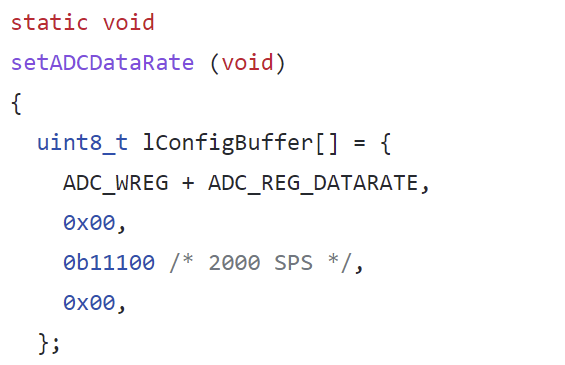
    The only configuration register I write to, apart from channel selection, is the one for data rate:

    Main schematic:

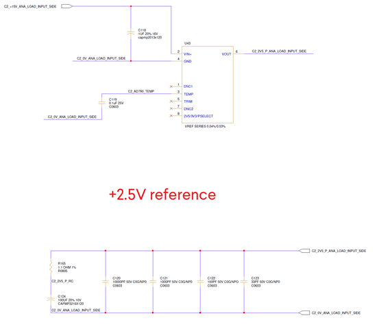
    +2.5V:


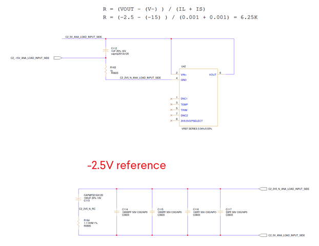
    -2.5V:

    Relays:

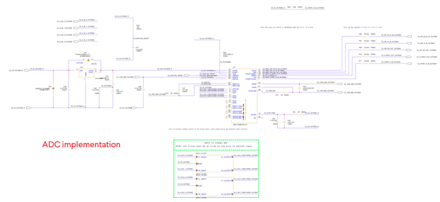
    ADC implementation:

  • We changed our firmware to enable PGA with a gain of 1 for single-ended readings, and the bug persists so far.

  • Hi Kevin,

    You might try using the internal reference to see if that makes any difference.  From the schematic you have a rather complicated setup and debugging can be difficult.  I would double check that all of your components can handle operation at the higher temperatures.  This would include the supply components, reference, relays and microprocessor to name a few.  The reason being that many components are only rated to 70 deg C (as opposed to 85, 105, or 125 deg C).  This would include many microprocessors.  The ADS124S06 is rated to 125 deg C, but any other components that connect to the device can degrade the operation of the ADS124S06.

    Best regards,

    Bob B

  • Hi Bob,

    I think we found the issue but I would like to validate something with you. What is the maximum SPI clock speed that the device can handle?

    We used to use 4MHz, but we figured that with temperature, the internal clock frequency of the ADS124S06 drifts and becomes dangerously low compared to the SPI clock, to the point where we see errors happening on the MISO line (the ADC response with the values).

    When we use a lower SPI clock frequency (e.g. 2MHz), we don't see the issue happening.

    Regards,
    Kevin

  • Hi Kevin,

    The SPI timing is as given in the datasheet in section 7.6.  The SPI can operate to 10MHz throughout the device operating temperature range.  That said, I know many customers have had issues with higher SPI clock speeds due to PCB layout.  If the SCLK passes through vias, there can be added inductance causing phase delays in the communication.  There can also be some ringing on the SCLK with overshoots and undershoots that may also cause some issues.  Usually many of these types of issues can be resolved by slowing down the SCLK.

    Best regards,

    Bob B