This thread has been locked.

If you have a related question, please click the "Ask a related question" button in the top right corner. The newly created question will be automatically linked to this question.

ADS131M08:

Part Number: ADS131M08

Hello,

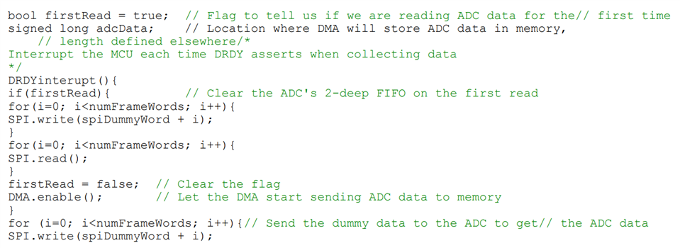
I have a technical question about the use of the ADC chip ADS131M08. I am using the SYNC input pin to start the conversion but then I have to perform 2 dummy reads before the data is available from the FIFO, I have read that this is not really the right way to use the SYNC pin, its not intended to be used as "Start Conversion" is that correct?  Also is there a way of disabling the FIFO, so that once DRDY pin output goes low, then I can read the data available immediately? I am operating in Continuous Mode.

Just to add, although I'm using this in continuous mode, I do pulse the SYNC input low to synchronize for every sample I need, then I wait for DRDY to go low then I read the data. The reason I do this is because I need to adjust the rate slightly of my sample period and i intended to do this by the SYNC pulse. Perhaps its better for me to do this adjustment by varying the CLK input frequency slightly and not pulsing the SYNC input every sample. (I've set the OSR to 128 and my crystal is 8MHz).

Kind Regards,

Phil Spanton

  • Hello Phil,

    I don't think I know exactly what you want to do, feel free to clarify.

    When you toggle SYNC and it lines up with an internal clock that matches the data rate, there's no action taken by the device. If you strobe SYNC, or quickly toggle SYNC so it doesn't line up, then the FIFO will be cleared. You either need to strobe SYNC or quickly read twice to clear out the FIFO. The FIFO also cannot be disabled. You don't need to do this for every sample, only if you miss a couple of conversions or pause reading samples and FIFO is full or backed up. If its empty, and nDRDY toggles low, read once and grab the data.

    If you don't monitor this ADC that often but want to minimize the time needed to read data when the ADC is needed, then there's really nothing to do besides clearing the FIFO and waiting for nDRDY to toggle again. Because it is not a conversion start, there's no way to get data immediately after clearing the FIFO (outside of timing the 2nd read to complete right before nDRDY toggles...).

    Yes, the best way to adjust the sample rate is to adjust the clock frequency out of the norm.

    Best,

    -Cole

  • Hello Cole, 

    Firstly thank you for coming back to me.  Just to briefly to clarify a bit more about what I am trying to do.

    I wish to continuously sample at a rate of approximately 16ksps, but I will need to vary the sample rate by some +/- 10%. I am looking at using an OSR of 128 (or even possibly 256) with an external clock nominally of 8MHz. These are only approximate values to give you an idea of what I'm trying to achieve. Currently the 8MHz clock source is from a crystal and I cannot vary it at the moment, so the thinking was to set the OSR =128 which should convert in time and pulse the SYNC pin low to start the conversion again, I believe though I have misunderstood the function of the SYNC pin. I do not have time to perform 2 dummy reads in each sample. Could you clarify two things for me please as follows:

    1) When you say quickly read twice to clear out the FIFO, do I have to still read 10 words (24 bit words in my case) twice or is there a quicker/shorter way of doing this ?      .          

    2) So is it possible that I can pulse the SYNC pin low for my every sample to reliably clear the FIFO, then immediately read after, if so what is the pulse width I need do this (when considering my above conditions) ? 

    Kind Regards,

    Phil Spanton

  • Hello Phil,

    Okay, thanks for the clarification.

    1)...[Do] I have to still read 10 words (24 bit words in my case) twice...?

    The short answer is yes, you'll need to read everything. The response and all channel data must be read twice. You can skip the CRC however. This is confirmed in the datasheet section 8.5.1.11 Short SPI Frames.

    "Quickly" is a bit relative but I think fair when comparing 16kSPS datarate vs. 25MHz SCLK, I think its fair. Not sure what SCLK you're running SPI at.

    2) So is it possible that I can pulse the SYNC pin low for my every sample to reliably clear the FIFO, then immediately read after, if so what is the pulse width I need do this (when considering my above conditions) ? 

    Correct me if I'm wrong, but it looks like you continually plan on collecting data from the ADC. There will be very few pauses. The only unique process you want to implement is variably change the data rate while the ADC is running, which you can do with the external clock like we talked about.

    If everything I said above is true, then I think we need to talk about FIFO again. I tried to explain earlier that we really don't need to drop the SYNC pin low for the sake of clearing the FIFO if we are reading every single conversion. If you want to synchronize SYNC to something, then sure, you're using it correctly and we can talk about the width. Otherwise, strobing SYNC to clear the FIFO is only needed on the first read. Here's some code in the datasheet that helps illustrate that point:

    Just replace SPI.write(spiDummyWord + i); with StrobeSYNC(); //To Clear ADC's 2-deep FIFO. As you can see, the firstRead; is cleared and we won't need to clear the FIFO anymore. Hopefully that makes sense. And I apologize if this is something you already know, its just that your question states "pulse sync low every sample to clear FIFO" which does not need to be done if you actually want to read consecutive conversions with no pauses.

    As for timing of SYNC to trigger a resynchronization event to clear the FIFO, just need to keep SYNC low for >1 t_CLKIN keep it high just as long, and then drop it low again so that this whole process is less than the data rate. Nothing too special there.

    Best,

    -Cole

  • Hello Cole, 

    Thank you for your explanations.

    I have one last question to ask, please find attached timing screen grab from my logic analyser monitoring some of the key signals.

    My external crystal = 8MHz, OSR = 256 which should give me a Conversion Rate of 15.625 ks/s, which it does after approx 2.5ms in, as shown in the attachment. You can see the single SYNC low pulse at the start which is approx 1us. The conversions start with the DRDY giving additional pulses and the result halves the expected sample rate. I use an interrupt which fires on the falling edge of DRDY signal, when I receive the interrupt I read the data. My SPI clock rate is 13.5MHz. One thing I forgot to mention before, although I have only spoken about just one ADC, I have in fact 5 ADC's on the board all driven from the same SYNC signal, they all need to be sampling together.    

    I have read in the data sheet that this could be due to me not reading the whole frame correctly but I can't see any evidence of this. Have you any ideas why I am seeing this please?

    Many thanks,

    Phil Spanton


  • Hi Phil,

    Yes, seeing half the expected data rate is a common issue related to everything we've been talking about.

    I know you haven't shown a zoomed in version of the the SYNC signal but what I imagine happened is that the SYNC pulse didn't trigger a resynchronization action and the FIFO continued to be full. This is under the assumption that you are reading every nDRDY toggle like you say. It could be fair that the whole SPI frame isn't being completed as expected and that causes one of the channel's FIFO to remain full. In the context of having multiple ADCs, using the SYNC is definitely the way to go.

    Either way, I think once you figure out how to properly clear the FIFOs on all of your ADCs, all of these issues will go away. One debug step I encourage you is to send a NULL command or read the STATUS register and ensure F_RESYNC is 1b after reading the next data that pops out after SYNC toggles.

    Best,

    -Cole

  • Hi Cole,

    Thank you once again for your answers.

    Is it possible that the ADC will function correctly if I have a gated clock approach (see diagram below) for the control to the CLKIN input pin. So I would, for example (for OSR =128), provide 256 clock periods on CLKIN, then disable the clock, read the data over SPI. After after a defined time I re-enable the clock to start the next conversion, this way I am controlling the Enable pin in order to determine where the conversion is started. Would this work?    

    Kind Regards,

    Phil Spanton

  • Hey Phil,

    This is a cool idea, we don't have a lot of info in the datasheet with what's going to happen when the device is powered but CLKIN is absent. Let me talk with the team and see if this is a viable use case for the device.

    Best,

    -Cole

  • Hi Cole, Yes if you could please clarify that would be great.

    Thank you for your continued support.

    Phil

  • Hi Cole,

    Do you have any feedback from the team at all regarding the gated clock idea?

    Kind Regards,

    Phil. 

  • Hey Phil,

    Still working on it, I'll keep you updated. Expect another response from me before the end of Monday at the latest.

    Thanks,

    -Cole

  • Hi Phil,

    Alright, so the short answer is: this might work. But you'll need to be pretty strict with the timings.

    Now I need to give the long answer.

    Intro

    Inherently, delta-sigma ADCs average which makes precise timing measurements that start and stop inherently challenging. SARs have much less difficulty doing this. A typical question from those learning about delta-sigmas is: when does the conversion start and end? The short answer to that is, as soon as nDRDY toggles low.

    ADS131M0x and conversion timing:

    For simplicity, when CLKIN goes low on the ADS131M0x, the conversion is "paused". The filters are not flushed, and we stay in the middle of the conversion. Hopefully you can see why this is a problem if you happen to disable the CLKIN in the middle of a conversion and the averaging is pause from one data point to another. This is mitigated if you can disable the clock at the end of a conversion, or as soon as nDRDY toggles low.

    The other note is that the SINC is an order 3 filter so you still might get invalid data for the first 3 or 4 data points.

    Also, you can access the device with SPI while the CLKIN is low, so no issue there.

    Going back to SYNC for a second:

    So at the end of the day, we're still dependent on nDRDY starting up at the same time as the other ADCs for this to work. And again, the only way we can do that is through SYNC/RESET.

    I know your goal is to have everything at the same time and you want to also change the data-rate by changing the clock. Strobing (not toggling at the rate of the data rate) SYNC results in one of two results:

    • Clock and nDRDY don't match up, the device resynchronizes and the conversion does restart
    • Clock and nDRDY do match up for the first toggle, but then don't match up for the second toggle and the device resynchronizes.

    So CLKIN is your determining factor whether all the ADCs are synchronized are not. Is having a maximum of a clock period delay good enough for your system? 

    Maybe we need another device:

    Delta-sigmas average, and SARs don't. Are we sure a delta-sigma is what you need or can a SAR get you the performance you want?

    Perhaps if you have more information on your project's specifications or what your end application is, we can help there. For example, the ADS131M0x was specifically designed for electronic metering, circuit breakers, metrology, and battery test equipment.

    Sorry for the delay, took awhile to get all the information!

    Best,

    -Cole

    Edit: forgot about SPI

  • Hi Cole,

    Much appreciate your support on this.

    We are stuck with the current design using these ADC's, we will now prototype various solutions for the gated clock as discussed, firstly using a PWM generator from the onboard STM32F756 and also in parallel our HW guy is looking at an external HW solution using a 8.192MHz clock and gating it for 256 cycles.

    Kind Regards,

    Phil.