Other Parts Discussed in Thread: ADS131E08, TMS320C6678
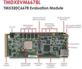
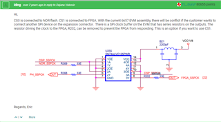
I am using ADS131E08 to communicate SPI with TMDSEVM6678LE.
I am using ADS131E08 to communicate SPI with TMDSEVM6678LE.
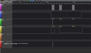
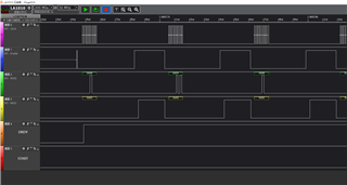
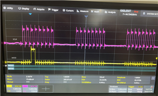
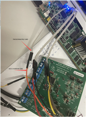
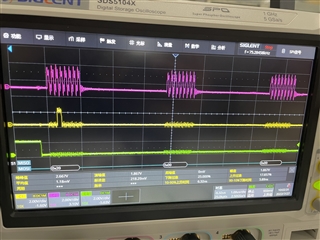
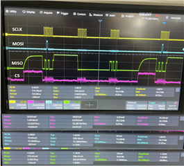
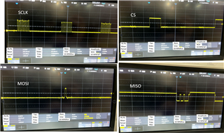
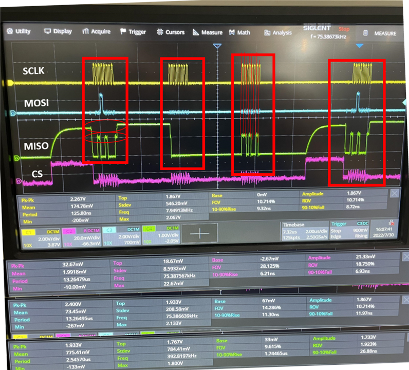
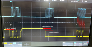
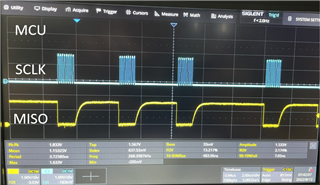
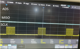
When I measure THE DIN at port J1 on the EVM, I can see the data being sent.
However, when I measured the DIN pins of THE ADS131E08, I found the waveform error.
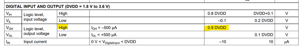
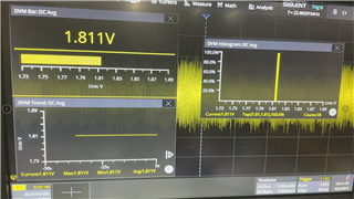
DVDD of EVM is 1.8V, SPI output voltage of 6678LE is also 1.8V, the digital level of both should be compatible, but why the DATA at the DIN pin of ADS131E08 is wrong?
(Channel 2 measures DIN on the J1 pin on the EVM.Channel 5 is the DIN pin for measuring ADS131E08.)