This thread has been locked.

If you have a related question, please click the "Ask a related question" button in the top right corner. The newly created question will be automatically linked to this question.

ADS1158: ADS1158 DRDY pin not going LOW

Part Number: ADS1158
Other Parts Discussed in Thread: ADCPRO

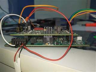
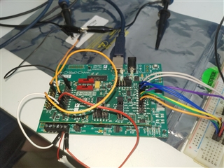
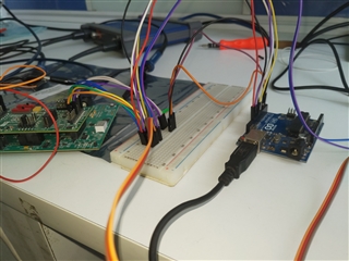
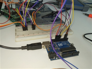
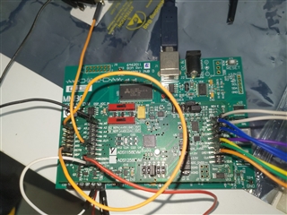
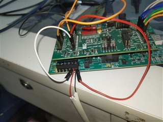
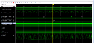
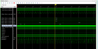
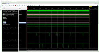
I am trying to control ads1158 module with a arduino, and i have tied the START pin to high, i want to use it in "channel read command" and "auto-scan mode",  but the current problem i am facing is that the DRDY remains HIGH all the time when the device is powered-on. i am using the device in default configuration. Please guide me.

Thankyou

  • Hi Harsh Gola,

    What is the state of the START pin when you turn on the ADC? If the START pin is high, the DRDY pin should toggle at the default data rate, even before you write any registers (assuming PWDN and RESET are also both held high)

    If this does not happen, then there is an issue with the supply voltages being provided to the ADC, or the clock provided to the ADC is not functioning.

    Please check that these inputs are correct before proceeding.

    -Bryan

  • Hi Bryan,

    Right after i power up the ADC , start pin remains LOW, after that i tie START, RESET, PWDN to 5v, but DRDY still remains HIGH(3v3).

  • Hi Bryan , 

    This is the code that i am using on arduino:

    #include<SPI.h>
    uint8_t reg1, reg2, reg3, reg4, reg5, reg6, reg7, reg8 ;


    void setup (void)


    {

    Serial.begin(115200); //Starts Serial Communication at Baud Rate 115200

    // pinMode(7, OUTPUT);//start//pulse conver is used
    pinMode(9, INPUT);//drdy
    pinMode(8, OUTPUT);//reset // tied to 5v 
    pinMode(6, OUTPUT);//pwdn //tied to 5v
    //digitalWrite(7,LOW);
    SPI.begin(); //Begins the SPI commnuication


    }

    void loop(void)

    {

    for(int i = 0 ; i <6 ; i++)
    {
    Serial.println(i);

    //////////////////////////////////
    digitalWrite(SS,LOW);delay(5); //toggle the ss signal to reset the spi interface as per ads1158 datasheet
    digitalWrite(SS,HIGH);

    digitalWrite(SS,LOW);

    delayMicroseconds(1);
    SPI.transfer(0x40);
    byte config0 = SPI.transfer(0);
    Serial.print("config0:");Serial.println(config0,HEX);
    digitalWrite(SS,HIGH);
    delay(1000);

    digitalWrite(SS,LOW);delay(5); //toggle the ss signal to reset the spi interface as per ads1158 datasheet
    digitalWrite(SS,HIGH);
    digitalWrite(SS,LOW);
    delayMicroseconds(1);
    SPI.transfer(0x41);
    byte conf1 = SPI.transfer(0);
    Serial.print("config1:");Serial.println(conf1,HEX);
    digitalWrite(SS,HIGH);
    delay(1000);

    digitalWrite(SS,LOW);delay(5); //toggle the ss signal to reset the spi interface as per ads1158 datasheet
    digitalWrite(SS,HIGH);
    digitalWrite(SS,LOW);
    delayMicroseconds(1);
    SPI.transfer(0x42);
    byte MUXSCH = SPI.transfer(0);
    Serial.print("MUXSCH:");Serial.println(MUXSCH,HEX);
    digitalWrite(SS,HIGH);
    delay(1000);
    //////////////////////////////////////////
    digitalWrite(SS,LOW);delay(5); //toggle the ss signal to reset the spi interface as per ads1158 datasheet
    digitalWrite(SS,HIGH);
    digitalWrite(SS,LOW);
    delayMicroseconds(1);
    SPI.transfer(0x43);
    byte muxdif = SPI.transfer(0);
    Serial.print("muxdif:");Serial.println(muxdif,HEX);
    digitalWrite(SS,HIGH);
    delay(1000);
    //////////////////////////////////////////////
    digitalWrite(SS,LOW);delay(5); //toggle the ss signal to reset the spi interface as per ads1158 datasheet
    digitalWrite(SS,HIGH);
    digitalWrite(SS,LOW);
    delayMicroseconds(1);
    SPI.transfer(0x44);
    byte muxsg0 = SPI.transfer(0);
    Serial.print("muxsg0:");Serial.println(muxsg0,HEX);
    digitalWrite(SS,HIGH);
    delay(1000);
    //////////////////////////////////////////////
    digitalWrite(SS,LOW);delay(5); //toggle the ss signal to reset the spi interface as per ads1158 datasheet
    digitalWrite(SS,HIGH);
    digitalWrite(SS,LOW);
    delayMicroseconds(1);
    SPI.transfer(0x64);
    SPI.transfer(0x01);
    delay(1000);
    /////////////////////////////////////////////
    digitalWrite(SS,LOW);delay(5); //toggle the ss signal to reset the spi interface as per ads1158 datasheet
    digitalWrite(SS,HIGH);
    digitalWrite(SS,LOW);
    delayMicroseconds(1);
    SPI.transfer(0x45);
    byte muxsg1 = SPI.transfer(0);
    Serial.print("muxsg1:");Serial.println(muxsg1,HEX);
    digitalWrite(SS,HIGH);
    delay(1000);
    /////////////////////////////////////////////
    digitalWrite(SS,LOW);delay(5); //toggle the ss signal to reset the spi interface as per ads1158 datasheet
    digitalWrite(SS,HIGH);
    digitalWrite(SS,LOW);
    delayMicroseconds(1);
    SPI.transfer(0x65);
    SPI.transfer(0x00);
    digitalWrite(SS,HIGH);
    delay(1000);
    /////////////////////////////////////////////////
    digitalWrite(SS,LOW);delay(5); //toggle the ss signal to reset the spi interface as per ads1158 datasheet
    digitalWrite(SS,HIGH);
    digitalWrite(SS,LOW);
    delayMicroseconds(1);
    SPI.transfer(0x46);
    byte sysred = SPI.transfer(0);
    Serial.print("sysred:");Serial.println(sysred,HEX);
    digitalWrite(SS,HIGH);
    delay(1000);
    //////////////////////////////////////////////////
    digitalWrite(SS,LOW);delay(5); //toggle the ss signal to reset the spi interface as per ads1158 datasheet
    digitalWrite(SS,HIGH);
    digitalWrite(SS,LOW);
    delayMicroseconds(1);
    SPI.transfer(0x47);
    byte gpioc = SPI.transfer(0);
    Serial.print("gpioc:");Serial.println(gpioc,HEX);
    digitalWrite(SS,HIGH);
    delay(1000);
    //////////////////////////////////////////////////
    digitalWrite(SS,LOW);delay(5); //toggle the ss signal to reset the spi interface as per ads1158 datasheet
    digitalWrite(SS,HIGH);
    digitalWrite(SS,LOW);
    delayMicroseconds(1);
    SPI.transfer(0x48);
    byte gpiod = SPI.transfer(0);
    Serial.print("gpiod:");Serial.println(gpiod,HEX);
    digitalWrite(SS,HIGH);
    delay(1000);
    /////////////////////////////////////////////////////
    digitalWrite(SS,LOW);delay(5); //toggle the ss signal to reset the spi interface as per ads1158 datasheet
    digitalWrite(SS,HIGH);
    digitalWrite(SS,LOW);
    delayMicroseconds(1);
    SPI.transfer(0x49);
    byte id = SPI.transfer(0);
    Serial.print("id:");Serial.println(id,HEX);
    digitalWrite(SS,HIGH);
    //////////////////////////////////////////////////////////
    delay(1000);

    while(1)
    { digitalWrite(SS,LOW);delay(5); //toggle the ss signal to reset the spi interface as per ads1158 datasheet
    digitalWrite(SS,HIGH);
    // digitalWrite(7,HIGH);//start high
    delay(100);
    //////pulse convert command
    digitalWrite(SS,LOW);
    // delayMicroseconds(1);
    SPI.transfer(0x80);
    byte pulse = SPI.transfer(0);/////////////////////
    Serial.print("pulse=");
    Serial.println(pulse, HEX);
    digitalWrite(SS,HIGH);
    // SPI.transfer(0x00);
    if (digitalRead(9)==LOW)//drdy
    {
    digitalWrite(SS,LOW);
    // delayMicroseconds(1);
    SPI.transfer(0x30);
    reg1 = SPI.transfer(0x00);
    reg2 = SPI.transfer(0x00);
    reg3 = SPI.transfer(0x00);
    reg4 = SPI.transfer(0x00);
    // digitalWrite(2, LOW);
    // dataF=reg2*pow(2,16)+reg3*pow(2,8)+reg4;
    Serial.print("Stat=");
    Serial.println(reg1, HEX);
    Serial.print("msb=");
    Serial.println(reg2, HEX);
    Serial.print("lsb=");
    Serial.println(reg3, HEX);
    Serial.print("reg4=");
    Serial.println(reg4,HEX);
    // Serial.print("finalData=");
    //Serial.println(dataF, HEX);
    // }
    digitalWrite(SS,HIGH);
    // delay(1000);
    }
    }}}

  • The ADC module is powered via J5A jumper with 5v, 3v3, 1v8 voltages. AINCOM is grounded, J6A-4 is grounded, EREFP is 5v, EREFN is 0v,  Sine wave input at AIN0 channel (auto scan mode).

  • Hi Harsh Gola,

    You should be using either 1.8V or 3.3V, I am not sure why you have both connected. Can you send me some pictures of the new hardware configuration? Please provide as much detail as possible

    Can you make sure that PWDN, START, and RESET are tied to 3.3V, then power up the ADS1158 EVM daughtercard. You can even disconnect the controller for this test. When the ADC powers up, the DRDY should toggle at the data rate. If DRDY does not toggle, it just stays high, then there are issues with the power supply or the clock.

    Let me know what happens, and please send pictures

    -Bryan

  • Hello Bryan,

    I thankyou for your continuous support, I have attached some pictures of the board, please check, i have tied RESET, PWDN, UNIPOLAR/POLAR pins to HIGH(5v from arduino, should i tie them to 3v3 instead?), EREFP is tied to 5v EREFN is tied to GND, and START pin is open, since i decided to use Pulse Convert Command(because setting the START pin did not result in activity on DRDY pin). In the above code i am sending 0x80 then checking the DRDY for LOW condition, then sending 0x30 and additional 0x00 0x00 0x00 to capture STAT , MSB , LSB byte. The registers I changed are muxsg0 (set to 0x01), muxsg1(set to 0x00) every other register is set to default.        

  • hello bryan,

    update :- i found the jumper on the ads1158 board , jumper J6 , it had G0 and ST pin shorted(found this on another forum), I have now changed it to short J6-1 and ST, now the DRDY pin is pulsing and it should when it set the START pin high. Now i am changing the arduino code to set START pin high initially, then check DRDY for LOW and send (0x30)(0x00)(0x00)(0x00) to retrieve the channel, i will update asap about the channel data i am receiving.

    FLOW:- 

    1.set RESET, PWDN, UNIPOLAR, START pin high (5v, should i tie it to 3v3 instead?)

    2.set configuration registers

    3.read back those registers

    4. check DRDY for LOW , then send (0x30). and stay in this state.

    Please check if i am taking the right approach.

    thankyou.

  • Hi Harsh Gola,

    You should tie RESET, PWDN, and START to whatever voltage you use for DVDD. There is a level translator between DVDD and the 3.3V voltage used for the digital communication, so you do not necessarily need to use the same voltage as the FPGA IO. However, it probably makes sense to use 3.3V for all of the digital IO voltages. PWDN and RESET already have pull-ups to 3.3V (R8 and R9) on the EVM. You would likely need to manually connect the START pin to DVDD because when you connect J3-1 and J3-3 together, there is a pull-down on this trace (R14). So you will need to make sure that you set START high in order to begin conversions, but the pictures you sent don't have a connection to the START pin on J6 (J6-1). Review the ADS1158EVM schematic for more details about how the EVM is designed.

    The pin to control the AVDD supply voltage (unipolar vs bipolar) can just be left unconnected, it is automatically pulled high in this configuration = set to unipolar.

    Also, I would recommend disconnecting the ADS1158EVM daughter card from the MMB0 motherboard, and applying power directly to the J5 header on the ADS1158EVM. There might be some contention between the controller on the MMB0 and your external controller

    If you want to use the channel data read command, then the process you outlined is correct: check DRDY for LOW and send (0x30)(0x00)(0x00)(0x00) to retrieve the channel data. Note that the first byte after the command is clocked in is the STATUS byte, and that this is only valid in Autoscan mode.

    -Bryan

  • Thankyou Bryan for your Guidance, I have attached some images of the results i am getting, please check and let me know if you need more detailed images, currently i am using one channel (AIN0) for testing, i want to use 7 channels ultimately(AIN0-AIN6)(Single-ended), the ADC is running on default configuration, i have only overwritten the muxsg0(0x01) and muxsg1(0x00) register to select the in put channels. i am using RESET, PWDN, START, DRDY, CS,MOSI, MISO,SCLK pins in total , adc is powered without the motherboard now, i provided a sine wave as input and result is noisy. in my current code i write muxsg0 and muxsg1 then take start pin from low to high, then start checking drdy for low and then send (0x30000000) to retrieve the channel data. please guide as to how can get the result with less noise.

    Thankyou


  • Hi Harsh Gola,

    Do I understand correctly that you are now able to successfully read and write registers on the ADS1158? So there are no issues performing these functions anymore?

    I ask because I do not see SCLK ("sclk_0") toggling in the screen captures you sent, so I am not sure what you are doing in these images.

    Now the only issue is that your sinewave input is noisier than you expected? The ADS1158 might not be the best choice for AC signals due to the way that delta-sigma ADCs sample an input. This might be better suited for a SAR ADC, unless you are measuring a very low frequency sinewave (<1 kHz). If you can provide more information about what signals (amplitude and frequency) you are trying to measure we can make better recommendations

    You can also check the noise performance of the ADC by shorting the inputs together and measuring the resulting noise. You can short the inputs together by choosing the same channel for both the positive and negative ADC inputs. This has to be completed in fixed channel mode using the ADS1158.

    Also check the noise performance against a known DC input, e.g. 2.5V from a precision source (you can use the reference voltage for the ADC for example). Assuming no other noise sources are present in your system, the noise measuring this constant 2.5V should be on the order of the ADC quantization noise (2*1.0666*VREF / 2^16, assuming no gain)

    -Bryan

  • Hello Bryan,

    i am able to read and write registers successfully, i am using this adc to measure data from sensors like, humidity, water pressure, temperature and water flow. i have attached some images , one showing spi communication, other showing the data i am receiving.  you might notice , it is mentioned in the sheet , that the NEW bit represents new Data, so i have separated the data in to two , one where i am collecting New and Old data, named, ads_1158_interface_ 0_channel_n (n= 0,1,2,3,4,5,6), and one where i am collecting only New data and discarding Old data, named, ads_1158_interface_0_channel_n_new.

    but i am still getting spikes at uneven instances. The sensors connected currently are, a humidity sensor(channel 1), 2 water pressure sensors(channel 0 and 2), a 5v dc source(channel 3) ,a 2v 100hz sine wave(channel 5).

    SPI clock = 8mhz, SPI triggering whenever DRDY goes LOW.   channel 0 to 6 enabled on ADC , others are set to 0 (off), autoscan mode, channel data read command. 

    all register are at default value, except muxsg1 = 0x00.

  • Hi Harsh Gola,

    Can you help explain what "ds_1158_interface_ 0_channel_n (n= 0,1,2,3,4,5,6)" is showing? Are you measuring these signals directly? Or are you measuring the data on the DOUT pin and then plotting each channel separately?

    Those spikes look like noise, probably from a power supply or clock line that is coupling into the ADC somewhere. They could also be voltage spikes in the ground plane if you do not have a solid ground connection e.g. ground bounce. You should try checking all of these components and make sure they are functioning properly.

    -Bryan

  • Hello Bryan,

    ads_1158_interface_0_channel_n (where n is channel no.) represent the channel no. , e.g. ads_1158_interface_0_channel_0 shows AIN0 data, and ads_1158_interface_0_channel_0_new also shows AIN0 data except that it discards old data every time based on status byte's NEW bit, e.g. old data on AIN0 channel is shown as 0x08(StatusByte) MsbByte LsbByte and new data as, 0x88(stat byte) Msb Lsb.

    I am collecting all the data on the DOUT buffer of the SPI module then checking the STAT byte to get the channel info, and then plot them separately.

    i am currently using the ads1158 module without the motherboard , i have connected j6-4 ground to fpga and connected AINCOM to GND pin on the ads1158 module. i have also connected the ground of the sensors to the ads1158 module and fpga both.

  • Hi Harsh Gola,

    Have you tried checking the stability and voltage at your power supplies? Do they droop at all when you are sampling?

    Have you tried using an external reference voltage from a precision source to see if the noise decreases?

    For now, I would also only input a known DC voltage to test your circuit and diagnose the noise. There are too many variables when you start trying to measure sensors, etc.

    -Bryan

  • Hello Bryan,

    i am supplying 5v DC to the ADC from a dedicated Power Supply Unit, although it dops to 4.9 or even 4.7 , it does not drop to or go near 0v. 

    For external reference i have set S1 and S2 switches to AVDD and GND respectively.

    i am also supplying a steady 5v DC signal to just one channel but, i am still getting dips whose values even go as low as 0(on the analyzer window).

    but whenever i run the ADCPro software to double check if there is noise in the signal, it runs just perfectly.

    Registers configuration:-

    Config0 = 0x0a

    config1 = 0x83

    muxsch = 0x00

    muxsg0 = 0x01

    muxsg1 = 0x00

    i am fetching channel data whenever DRDY signal goes low.

    SPI clock  8 MHZ.

  • Hi Harsh Gola,

    If AVDD is dropping to 4.7V, this is below the recommended operating conditions of the ADC (AVDD must be AVSS+4.75V, and I assume you are measuring AVDD with respect to AVSS). This could cause a wide range of issues within the ADC, since the ADS1158 is designed to operate at effectively 5V AVDD.

    I would ensure that your power supply is very stable and does not droop. There is a chance this might not resolve your immediate issues, but it very likely could cause future challenges

    What is your IO voltage on the board? Is that supply drooping as well?

    -Bryan