A related question is a question created from another question. When the related question is created, it will be automatically linked to the original question.
If you have a related question, please click the "Ask a related question" button in the top right corner. The newly created question will be automatically linked to this question.
ADS131M04EVM: How to calibrate the ads131m04evm offset and gain of the ADC?
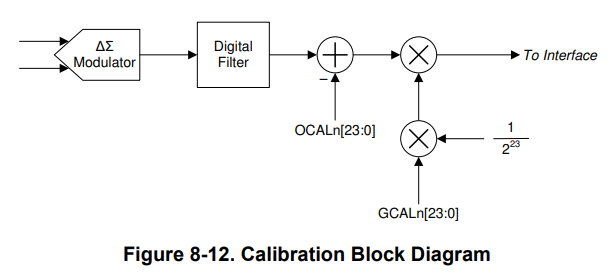
Please look at section 8.3.11 Calibration Registers in the ADS131M04 Datasheet.
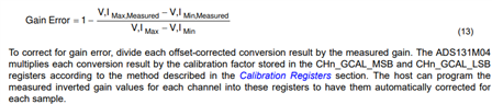
For a short summary, you'll be writing into 2 different registers: OCALn and GCALn. OCALn represents the offset and GCALn represents the gain correction.
As mentioned before, please check out the TIPL ADC videos I linked above. Here is a screenshot from the lesson:
As shown in the block diagram above from the datasheet section, the offset voltage is subtracted from the results so you simply need to write the code corresponding to the offset voltage into OCALn.
For GCALn, we have the procedure and equations in section 9.2.2.4 Calibration. There's also helpful info about OCALn. Here's a screenshot with the equation and general procedure for GCALn specifically.
There also might be something useful in the Example code, feel free to check it out:
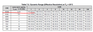
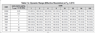
OSR@16384 GAIN@1, the effective resolution is 20.4, It will have 3.7 dead bits, and those dead bits will all turn into noise, right?
2^3.7 LSB becomes noise,converted to voltage is 1.89uV,right?
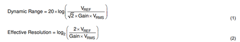
You are correct but there is one important concept I'd like to highlight. The concept of dynamic range and effective resolution are derived from noise, as shown in the datasheet and below:
So the noise table, Table 7-1, comes first and is measured on the ADC. Then we plug that into the equations above to get the specifications in the datasheet. So the table for that setting shows 1.9uV(RMS) and you calculated 1.89uV(RMS).
In other words, your math is perfect but it is a fundamental different perspective. The noise creates dead bits. Its pedantic but helps illustrate what is actually happening inside the ADC a bit more.
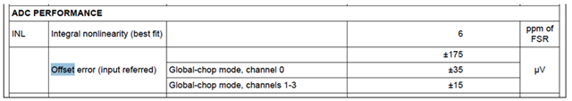
I noticed that the offset error of channel three is +/-15uV, is this the same parameter?
The +/- 15uV is a typical offset voltage that has nothing to do with noise. Offset is a DC error where noise relies on bandwidth (BW) and therefore, AC can be considered an AC error. When you were calibrating for offset, you should have noticed that the value probably fell within the +/-15uV if you translated codes to voltage.
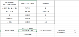
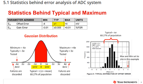
Anyways, the typical value is given as a range to help the user make statistical error decision based on the specification. You can learn more from the TIPL training video: 5.1 Statistics behind error analysis of ADC system. I've copied and pasted a very important slide about that discussion below.
But the voltage of about 15uV cannot be calibrated, how should it be calibrated?
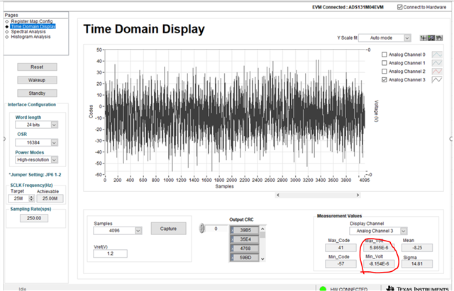
According to your screenshot, 15uV is in the units of Peak to Peak otherwise written as 15uV(pkpk). You might have noticed me write V(RMS) in the last response, most engineers like to discuss noise on context of the RMS value as statistics and the distribution (which you can get from the histogram tab of the GUI) show that getting the peak noise level is statistically unlikely where getting the RMS value is much more likely.
The quick rule of thumb for a gaussian distribution is that Vpkpk/8 = VRMS. So if I divide 15uV(pkpk)/8 = 1.875uV(RMS) which correlates to the noise specification that you were showing me earlier (f_data = 250SPS, G = 1). Alternatively, you should use the Mean value in your screenshot it, convert it to codes and you'll get a similar answer.
Other thoughts:
So far, every question of yours has been related to a TIPL video. I would highly recommend you watch those first and check the main FAQ for more learning:
When you were calibrating for offset, you should have noticed that the value probably fell within the +/-15uV if you translated codes to voltage.
Yes, this effect can be achieved after calibration in fact.
I'm in favor of using noise as a RMS value that is more normal and the mean value displayed by the host computer is also very small after calibration.
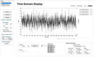
I have a question whether this Mean value is an average value or a RMS value? Then how can the customer's MCU get this value? Is there a corresponding register or what?
I have a question whether this Mean value is an average value or a RMS value? Then how can the customer's MCU get this value? Is there a corresponding register or what?
Good point, I misspoke earlier. The equation between RMS and mean and sigma (standard deviation) is as follows:
RMS^2 = Mean^2 + Sigma^2
So, if there was no DC error offset (or Mean = 0), then the standard deviation would equal the standard deviation. So, Sigma in the GUI is the noise in RMS, I'll edit my previous response. There's assumptions here that you successfully calibrated out DC error but it seems correct when I do the math.
All of the this is calculated in the GUI, so there's no registers for the customer to go and grab this information. Our GUI's use labview derived libraries and equations, if I'm not mistaken. The GUI grabs the raw ADC codes and then looks at all the samples and calculates this information. The MCU or processor of the customer would have to calculate this stuff on their own if they want it in their system but that isn't always needed at run time in a real system.
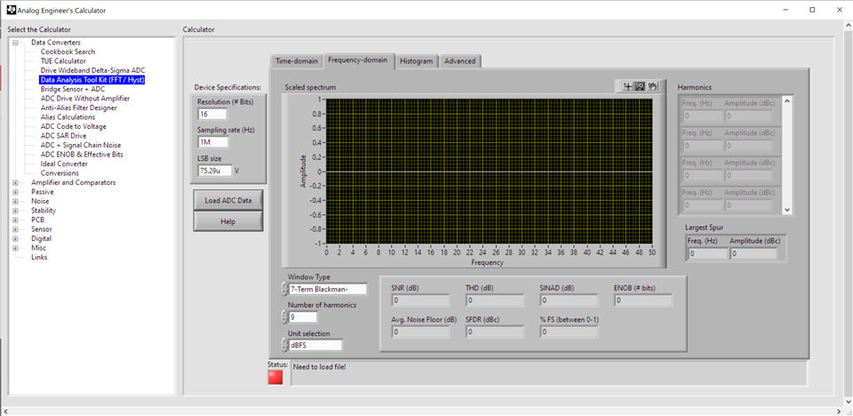
At this point, I'm confused what the needs are from the customer. If the customer wants to see the ADS131M0x performance in context of offset, then the GUI is good enough. If they want more calculations they can throw their data in the Analog engineer's calculator and take a look at noise floor, THD, SNR, etc. Or if they are good with MATLAB or labview, they can do it themselves with raw data collected from the GUI.
So, if there was no DC error offset (or Mean = 0), then the standard deviation would equal the standard deviation. So, Sigma in the GUI is the noise in RMS, I'll edit my previous response. There's assumptions here that you successfully calibrated out DC error but it seems correct when I do the math.
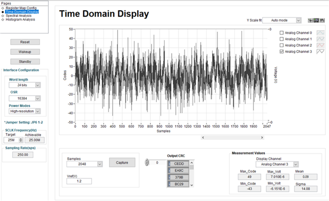
The mean can be calibrated very close to 0, but the standard deviation is still very large.
In this case, mean is 0.09 and sigma is 14.08.
Customer want to test accurately 10uV input signal, ADS131M04 can do it?
What parameters should we recommend customers to use?
At this point, I'm confused what the needs are from the customer. If the customer wants to see the ADS131M0x performance in context of offset, then the GUI is good enough. If they want more calculations they can throw their data in the Analog engineer's calculator and take a look at noise floor, THD, SNR, etc. Or if they are good with MATLAB or labview, they can do it themselves with raw data collected from the GUI.
Last time I confirmed with the customer that their MCU will process the data, but he is not clear how to deal with the customer.
I need to confirm again.
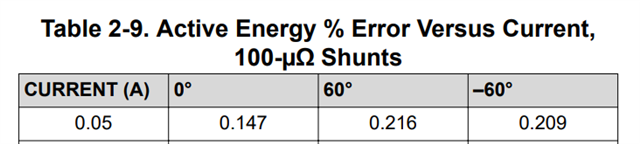
They use a shunt resistor on the input of the ADS131M04 and they're able to measure 50mA with 0.0625% accuracy.
Quick math shows they're measuring: 0.05*100*10^-6 = 5uV with 0.147% accuracy. So, yes, its possible and the TIDA-010036 had data to prove it. Note, e-metering has a pretty well known signal at 50/60Hz and their calibration process includes phase correction so it is in depth. I'm not sure how easy it will be for the customer's project.
The concept of dynamic range and effective resolution are derived from noise, as shown in the datasheet and below:
So the noise table, Table 7-1, comes first and is measured on the ADC. Then we plug that into the equations above to get the specifications in the datasheet. So the table for that setting shows 1.9uV(RMS) and you calculated 1.89uV(RMS).
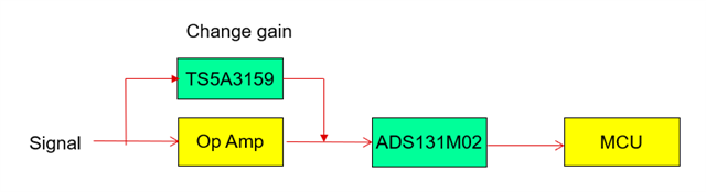
Hope you are all well. I have a question about the ADS131M02 PGA.
MCU sample input signal application
1. When the input signal normal, the signal delivery of the ADC may be amplified at 30 gain;

2. When the input signal is very small, we need to change switch and  get the signal amplified at 60 gain;


So my question is that when input signal is very small, I keep the gain of the op amp at 30 gain, then I adjust the gain of the ADC to 2, can this achieve the same effect?