This thread has been locked.

If you have a related question, please click the "Ask a related question" button in the top right corner. The newly created question will be automatically linked to this question.

ADS42JB46EVM: Setting M (# of converters)

Part Number: ADS42JB46EVM
Other Parts Discussed in Thread: ADS42JB49

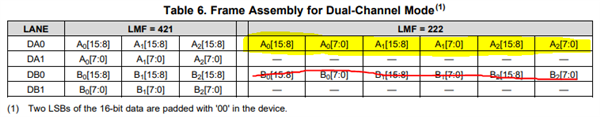
I am reading in my ILA sequence transmission that the M configuration bit is outputting 1, which, based on Table 9, means that there are 2 converters in operation. How do I set M=1 converter? I assumed that was set by changing if Channel A/B was powered down. I have powered down Channel B so I assume the ADC would correctly indicate in ILA that there is only one converter.

My desired setting of LMFS is 1121. I see that all the other configuration parameters are being transmitted correctly in ILA (with the exception of L which is configured for 2 lanes because M=1 instead of 0). I have attached my settings file below.

ADS42JB49_EVM_ST_0810.cfg

Though 1121 is not a listed configuration in the datasheet, it is valid based on this discussion: e2e.ti.com/.../4073194

  • Hi Sharon,

    An LMFS = 1121 can be achieved very simply by powering down Channel B while the ADC is configured for LMFS = 2221 mode. Simply configure the receiver to only expect the Channel A data, power down the ADC channel B, and there is no further action. 

    Regards, Chase

  • Hi Chase, 

    Thank you for the quick response. I am still receiving a link configuration parameters mismatch error on the receiver side. Right now, the ADC is transmitting LMFS = 2221. I have tried having the receiver set up as 1221 and 1121 but the receiver is looking for L=1 since I have the receiver designed to receive the DA0 lane only. How do you recommend I resolve this?

    Thanks.

  • Hello Sharon,

    The transceiver shouldn't have any problems with this 'LMFS=1121' mode. Are you using our TI JESD Rapid Design IP for Xilinx FPGA?

    Does the xcvr ip work when setup for LMFS=2221 and both channels on the ADC are running?

    Thanks, Chase

  • Hi Chase,

    I am not using a Xilinx FPGA so I am not making use of the TI JESD Rapid Design IP. My set up consists of the ADC EVM clock, sync, and DA0 lane wired to a non-Xilinx FPGA EVB. My ideal mode is LMFS=1121. 

    If I understand what you are suggesting -- you propose that I put the ADC in LMFS=2221 mode and power down channel B. I should then configure the FPGA to LMFS=2221 mode and ignore the data from the second lane (since nothing is being transmitted). 

    I have set up the ADC in LMFS=2221 mode with channel B powered down. I then set FPGA in LMFS=1221 mode and LMFS=2221 mode with the lane 0 & 1 inputs tied together and lane 0 output not going anywhere. Both still give me a configuration link parameter mismatch error.

    Is there a way to set up ADC in LMFS=1121 mode?

    Thanks, Sharon

  • Hi Sharon,

    There is no way to set up the ADC in LMFS=1121 other than powering down the ChB. I am suggesting to configure the FPGA to function in LMFS 1121 mode, not LMFS=1221 mode. I am wondering if the FPGA is expecting data on the second lane, which is not present with ChB powered down, and this is the configuration link parameter mismatch error. Which FPGA are you using?

    Regards, Chase 

  • Hi Chase,

    You can see my original settings in my original post. With that configuration [ChB powered down, 20x mode one lane per ADC], I then read the ILA data being transmitted and the ADC was transmitting LMFS=2221. It seems that the ADC is still assuming 2 converters (M) and communicating that to the FPGA. I would like the ADC to transmit LMFS=1121. What else needs to be changed in my settings?

    Thanks, Sharon

  • Hi Sharon,

    I'm checking with our team on this. I am more familiar with DAC side JESD, however my understanding is the transceiver decides the LMFS settings and so long as the selected settings are compatible with the ADC JESD settings, then there is no issue. Kindly await a response. 

    Regards, Chase

  • Thank you Chase. 

    I got it working under strange circumstances. Initially, I hacked the design so so one lane of data was fed to both lanes on the FPGA, which resulted in a link parameter mismatch error only on Lane 0 but not on Lane1. I then hooked up DB0 from the ADC to the FPGA and properly implemented a 2 lane FPGA design (Channel A0 to FPGA lane 0, Channel B0 to FPGA lane 1). With that configuration, I was getting link mismatch errors on both lines. I connected Channel B0 to Lane 0 on my FPGA and Channel A0 to Lane 1 on my FPGA and that fixed my problem. 

    Looking at the link parameters being sent in the second multi-frame, the match exactly except that Channel B's checksum is one less than Channel A. I don't know why they differ given that all other parameters are exactly the same. Is there anything else other than that second multi-frame that is being summed for the checksum? Also, Channel B is 8 bits (N'/2) slower than Channel A but my FPGA holds all parameters into a buffer until all lanes see the /R/ character so that shouldn't affect anything.

    I double checked that the connections between ADC <> FPGA are correct.

    I am still most interested in a LMFS=1121 scenario since that is my ideal implementation but I am also curious why adding another lane and swapping the lanes resulted in it working.

    I see that powering up or down Channel B still results in M=1 being transmitted so the "power down" register does not affect how many converters the ADC assumes is in operation.

    Thanks,

    Sharon

  • Hi Sharon,

    Apologies for the delay. I've received feedback from one of our FPGA experts, please see below comments:

    • Given that when the lanes are swapped between the ADCs, the design start to function is an indication of lane mapping mismatch. Is it possible they share the schematics with us?
    • The JESD checksum includes the lane number, meaning the different lanes will have a different checksum.
    • Additionally, it is possible to configure the FPGA for an LMFS of 2221 and simply disable the second lane corresponding to the powered down ADC channel.

    Regards, Chase