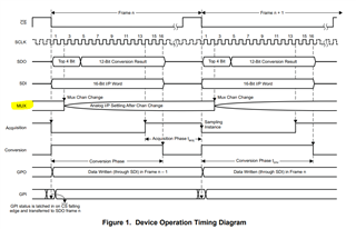
This thread has been locked.

If you have a related question, please click the "Ask a related question" button in the top right corner. The newly created question will be automatically linked to this question.

ADS7953: how to understand Tq?

Part Number: ADS7953

Tq is said to be 

Minimum quiet sampling time needed from bus Tri-state to start of next conversion.

1. How is it different from acquisition time?

2. Why acquisition time and conversion time could be overlapped? 

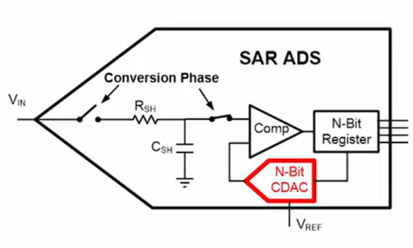
For SAR ADC, there is a sampling capacitor, during acquisition time, the cap should be connected to input pin, during conversion time, the cap should be unconnected to input pin, then my understanding is that the acquisition and conversion time could not be overlapped.

3. The acquisition time start from 14th clock and ends at next instance CS pulled from high to low. What if the duration is lower than 325ns requirement? What data could I get through SPI reading? Wrong data or previous conversion data?

  • Hello, apologies for the delay, there has been overlap on individuals being out of office 

    1. the acquisition time and the quite time can happen in parallel. The device is in acquisition time while the quite time is occurring, the quite time is simply a called out period of time for the device to be in tri state, which is not necessary true for acquisition phase

    2. this is a common question for this device; this is because of the mux functionality of the device in parallel with the conversion time length. the conversion time is a fixed time period based on the clock, note also when the mux changes channels. This allows for the the two time period to overlap, but also results in a 2 frame delay for measured data. 

    3. the minimum acquisition time is based on the max sampling rate, if the minimum acquisition time is not provided, i would suspect that other timing parameters may also be in violation. in general a shorter acquisition time results in a settling error at the input, resulting in an inaccurate measured output. 

    Regards

    Cynthia

  • For the second question:

    At acquisition phase, the left switch would be turned on and the right side switch would be turned off, and Csh will be charged to the same level as Vin.

    At conversion phase, the right switch would be turned on and the left side switch would be turned off.

    That's why I wonder how could these two phases could overlap.

    But it seems that the reply haven't answered my doubt.

  • I understand your question, but there is limits to what can be shared as to how the device functions. This device, as the datasheet states, "inherently includes a sample/hold function", but note that the information about the switching you indicated is not included. This is intentional, as the overlapping is a special characteristic of this device to achieve the max sampling rate. 

    Please note the previous response, and know that one conversion cycle is made up of a the acquisition phase and a conversion phase. 

    Regards

    Cynthia