This thread has been locked.

If you have a related question, please click the "Ask a related question" button in the top right corner. The newly created question will be automatically linked to this question.

ADS8167: Questions on the reference setup

Part Number: ADS8167

We are in the process of designing an instrument using the ADS8167. We do have a development board on order for testing, but would like some additional information which is not clear from the datasheet.

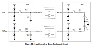
The input channels we are digitizing are AC and have the characteristic of saturating the front end (either + or - rail) during an output phase, and we will be sampling 8 channels as they come out of saturation and settle. The final stages feeding the ADS8167 multiplexer is a rail-to-rail single supply OpAmp, with drive capability of about 50 to 100 mV offsets from the rails. Our desire is to allow the full ADC range to be used on the unsaturated signal out of the final stage. We are considering running with the internal reference and use the REFby2 output to set the center voltage of the final stage. The AIN_CFG would be set for separate channels (0), COM_CFG set to 1 with AIN-COM wired to REFby2 for pseudo-differential operation, and the REFby2_MRG register would be set to provide an offset of ~100 mV (01100001b).

Are there any issues with this approach?


In order to save a regulator we are considering powering the final stage OpAmp from 5V (same as the ADS8167 AVDD) which would allow the ADC to see values close to 1V greater than Vref/2, instead of powering the OpAmp from Vref + 0.2V which would limit the ADC input (ADC-INP - ADC-INM) to Vref/2 + 0.1V (which appears allowable from the datasheet). This leads to the following questions:

  1. What happens if an input to the mux goes above Vref + 0.1V - is there crosstalk between the mux channels?
  2. What happens if the ADC attempts to read something above Vref/2 + 0.1V in pseudo-diff mode?
  3. Are we correct in assuming that the ADC will report inputs between Vref/2 and Vref/2 + 0.1V as 0xFFFF in pseudo-diff mode?
  4. Are we correct in assuming that the ADC will report inputs (ADC-INP - ADC-INM) between -Vref/2-0.1 and -Vref/2 as 0 in pseudo-diff mode?

Figure 22 in the datasheet shows Noise Performance vs Temp. Am I correct in assuming this is with the internal 4.096V reference? In Figure 24 a graph is shows noise with varying voltage, so I assume it has an external reference. However graph 24 seems to show worse noise at 4.096V when compared to the 25C point on Figure 22. Can you help me understand that?

Thanks, Chip Weller

  • Hello Chip,

    No concerns with your proposed configuration other than the offset value. In this case, I would suggest setting the REFby2_MRG register to 0x01010001b due to the tolerance of the margin offset (+/-10%).  The maximum for the AINCOM should be no more than Vref/2+0.1V.  At 10% worst case, this setting will still slightly exceed this recommendation, but you should still maintain good linear performance.

    Also, it is preferred to power the input amplifier from the same analog supply as the ADC.  The ABS maximum input range is limited by the input protection diodes, which clamp the input voltage between ground and the AVDD supply voltage.  As long as you do not exceed the AVDD supply voltage, there will not be any internal coupling between channels.

    1. What happens if an input to the mux goes above Vref + 0.1V - is there crosstalk between the mux channels?

    No crosstalk until the input exceeds AVDD.  The output code will simply saturate at + full scale.

    1. What happens if the ADC attempts to read something above Vref/2 + 0.1V in pseudo-diff mode?

    The output will read positive full scale.

    1. Are we correct in assuming that the ADC will report inputs between Vref/2 and Vref/2 + 0.1V as 0xFFFF in pseudo-diff mode?

    Yes, if ADC input (AINx-AINCOM) is greater than or equal to Vref/2-1LSB, then the output code will read 0xFFFF.

    If the AINCOM pin is connected to the REFby2, and set to Vref/2+0.1V, then your full scale input range on the AINx input (relative to ground) will be from 0.1V to Vref+0.1V.  At 0.1V (AINx relative to GND), the code will be 0x0000 and at Vref+0.1V (AINx relative to GND), the code will be 0xFFFF.  AINx equal to Vref will still be inside the full scale input range, and read approximately 0xF9C0.

    1. Are we correct in assuming that the ADC will report inputs (ADC-INP - ADC-INM) between -Vref/2-0.1 and -Vref/2 as 0 in pseudo-diff mode?

    Yes, this is correct.  Any differential voltage less than or equal to -Vref/2 will read as code 0x0000

    Regards,
    Keith Nicholas
    Precision ADC Applications