This thread has been locked.

If you have a related question, please click the "Ask a related question" button in the top right corner. The newly created question will be automatically linked to this question.

ADS8881: How to measure ENOB(DC) and PCB layout improvement

Part Number: ADS8881
Other Parts Discussed in Thread: OPA2330

Hello, I  encountered two problems when I using ADS8881 to have a test

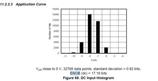
1  ADS8881 datasheet have a measurement for ENOB(DC) as the following displays(Page 39), how to measure it actually?

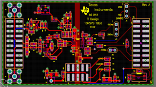
2  When I see TI's reference design for ads8881( DAQ_Low_Power_10kHz_AC_Verified.pcbdoc),I have an idea to improve its noise performance than ever before, First, we can use differential lines for analog chain, especially for Analog Input ,OPA2330. Secondly, we can decrease coupling between AGND and digital interface in 2rd GND layer. We can drill down the analogue ground below the second layer of digital interfaces, leaving only the analogue ground on the left.  I want to know whether my proposal is reasonable

  • Hello,

    1. There is a short blog about this topic available that I believe will be helpful here: Accuracy Part 1

    2. Signal chain improvements will always improve overall performance. As for the grounding, the ADC should use the same ground as the signal input chain. It is common to separate digital ground an analog ground. What I am understanding you are proposing is using one solid ground for all digital and analog circuits, which is also a common practice. If there are two layer grounds, then yes, these ground should have a solid connection between the two, such as having a ground stitching VIAS across the whole board connecting the two layers. This would be helpful. 

    Regards

    Cynthia