Hi experts,
I have some questions about DDC112Y. Could you please answer them?
[Environment] AD sample with CONV inversion in 0.5 seconds, RANG = 1, CLK = 10MHz, PHOTODIODE (S6429-01 made by Hamamatsu Photonics) in continuous mode.
- How to acquire time stability
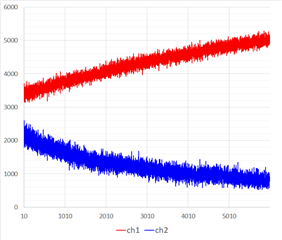
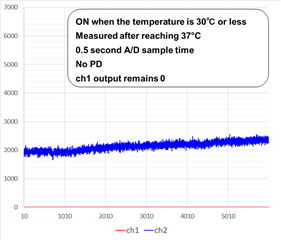
My customer attached a resistor of 1Mohm or 330kOhm to AIN pin instead of PHOTODIODE (S6429-01 made by HPK) in order to see the time stability (1 hour) of the ADC DDC112Y. However, the measurement result in that situation has much more noise than when PHOTODIODE is attached, and they can't not evaluate the stability of ADC.
Is it not possible to see the time stability of the ADC with resistance? Assuming that the resistance is useless, what kind of dummy load can be applied to evaluate the time stability?
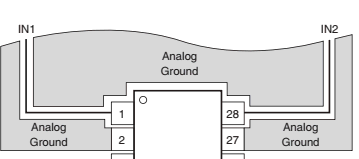
- Output when the input terminal is open, grounded, and grounded with a resistor
In the customer's measurement, when AIN is dropped to GND, it becomes 1048575 of FFFF. When opened, it becomes 0, but the data sheet P23 says that 4096 is output at 0.
Is it correct that it is FFFF when it is dropped to GND and 0 when it is open?
Best Regards,
Taito Takemura