This thread has been locked.

If you have a related question, please click the "Ask a related question" button in the top right corner. The newly created question will be automatically linked to this question.

ADS7952: Cannot read ADC channel values from SPI comms

Part Number: ADS7952

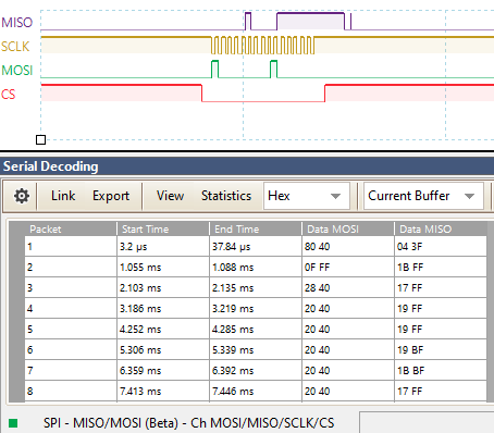
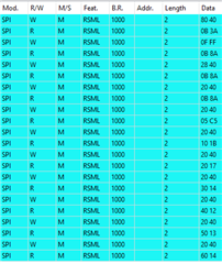
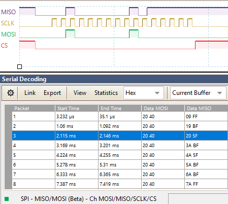
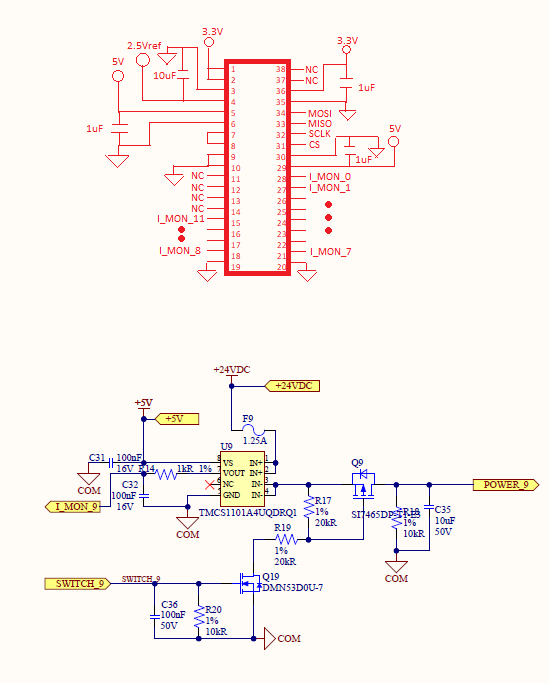
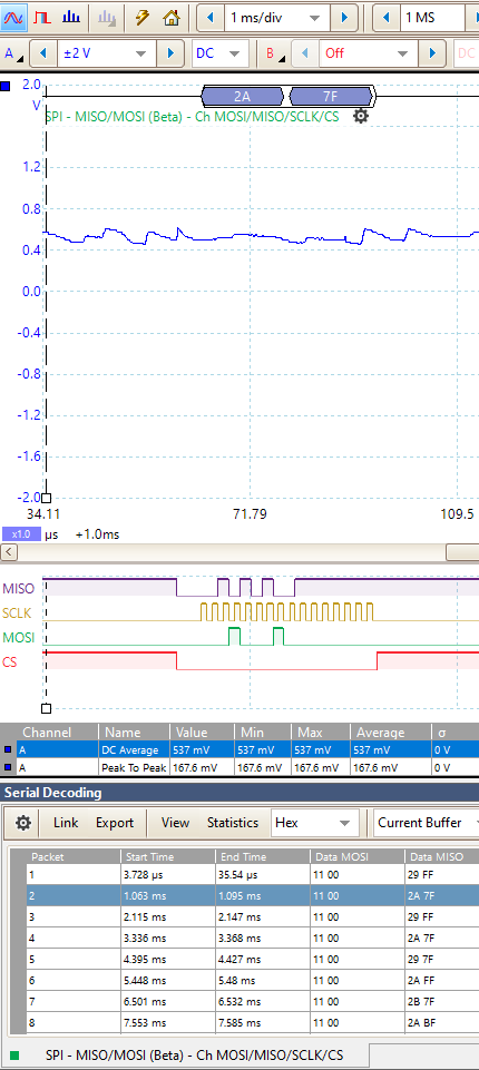
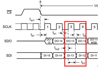
I have an ADS7952 connected to a PIC32MZ using SPI communication (3.3V IO) with all 12 channels connected to current monitor voltage outputs (0-5 V). For referance, the +VA = 5VDC; +VBD = 3.3VDC; Vref = 2.5VDC; MXO is tied to AINP; and we are using range 2 setting (2xVrev). I have tried setting it in manual and auto modes to output the 12 channel values but all the replies from the ADS7952 are 0x1BFF. the first byte is supposed to be an incrementing channel number but it doesn't seem to change. I tried sending manual requests for specific channels but the next frame is still 0x1BFF. Am i missing something that will fix the messages from the ADC?

  • Hi Julian,

    Welcome to our forums!

    There are a couple of things that I would like to address. The first being the SDO and SDI labeling. This looks to be in the point-of-view of the MCU correct? I would just like to be sure since the MOSI/MISO labeling looks to align correctly. 

    Second, the first command you are sending is 0x1000. This puts the device in manual mode but doesn't allow you to program DI06-DI00. You are then sending 0x0FFF right after. This will continue the device operation. My question here is if you meant to send 0x1000 first or did you mean to send 0x8000 to access the Auto 1 mode channel sequencing? 

    Additionally, did you make any previous right prior to the displayed 0x1000 at the top of the serial decoding window?

    Regards,
    Aaron

  • Hello,

    The SDO/SDI is from the view of the MCU. I had attempted manual mode previously and seemed to have forgotten to change the fist packet out to 0x8000. The image was the first couple data packets from startup, no previous writes prior to 0x1000. 

    I will change to code and reply with the results soon.

    Julian V 

  • Hi Julian,

    That is what I suspected. Thanks for the clarification! I will await your test results. 

    Regards,
    Aaron

  • I have corrected the code to output 0x8040 as the first command and i am seeing the same results for the response. i had also notice on the datasheet that pin 2 (GPIO3) is a active low power down pin so i pulled it high (3.3v) just in-case. This did not change the response.

    What would you suggest to get expected data from the ADC?

    Thanks,

    Julian V

  • Hi Julian,

    There is nothing wrong with the commands. I went ahead and performed a sanity check on an EVM using an I2C/SPI host adapter. You can see that the SDO data is increasing as the SDI commands are being sent. 

    However, I think there may be a communication error. This family of devices requires that there be 16 clock cycles but it looks like you are only sending 15. I am only counting 15 full cycles. Is it possible for you to provide one more clock cycle?

    Regards,
    Aaron Estrada

  • I count 16 falling edges and 16 rising edges within the CS frame. I am using the SPI protocol so i am not able to easily add or remove a clock cycle off of my intended message. 

    After looking at the timing diagram of the datasheet i noticed the SCLK was low during the CS falling edge. After changing the code's SPI settings to start low and transition on falling SLCK (sample on rising SCLK), I received a counting reply.

    At this point it appears to reply correctly but the value the ADC is reporting is not correct... i have 0.5V on each channel and the ADC is replying with a 0xABF most of the time (between 0x9BF and 0xAFF). according to this value the ADC is reporting 3.35V. Note in the image below i have captured the first 8 channels and i have pulled the 3rd channel (CH2) to GND but the ADC is reporting 0.116V.

    Thanks,

    Julian V


  • Additional note: i used a shorter GND wire to short the input channel and got 0x01F (0.038V). this confirms im getting data and grounding the input is near 0V but the ADC does not seem to match my measured value above 0V.

  • Hi Julian,

    Great that you can now communicate properly. There were 16 falling edges but it was not counting that initial falling edge as the first SCLK cycle starts at the first rising edge as far as the ADC is concerned. 

    Now switching attention to the output codes. I have a couple of questions:

    • Do you have a schematic to share? I would like to see what is driving the inputs as well as the circuitry around the ADC.
    • Have you verified the voltage at the AINP pin of the device as a sanity check?
    • Are the supply levels stable when using the device?

    Regards,
    Aaron Estrada

  • I accidently clicked the "this resolved my issue" instead of reply... can you undo that action?

    I created a redline schematic to share however it is build per the non-buffered example in the datasheet

    Below is a capture of manual mode displaying CH2 with the scope probe on MXO/AINP. The voltage is as expected ~0.5V. There is some noise on the line however it does not explain the 0xABF return value (even if the ref x 2 is not active, which it should be).

    The 5V, 3.3V and 2.5Vref voltage rails are all stable and have a Vp-p of <0.05V

    Thanks,

    Julian V


  • Hi Julian,

    I cannot undo the 'TI Thinks Resolved' status but the thread remains open so that is fine. 

    This is definitely puzzling. With SAR converters, there is typically some trouble presented with a voltage error due to improperly driving the ADC. However, I would not expect the error to be this large. The schematic looks fine and you measured directly at AINP which looks fine. I have a few more questions that I should have asked earlier:

    • What is your SCLK frequency?
    • What is the time from CS falling edge to first SCLK rising edge?
    • Your frame length looks lengthy but this is fine. When you are performing multiple reads/writes, what is the frame length?
    • Can you measure the th2 time (Hold time- Rising edge of SCLK to SDI valid)?

    Regards,
    Aaron Estrada

  • SCLK = 500kHz

    tsu1 (CS falling to first SCLK) = 3.73 us

    Our CS frame length is 35.5 us to send the 16 bit message on MOSI and receiving 16 bits at the same time on MISO. We send a frame every ~1 ms.

    th2 = 1us (data changes on SCLK fall which is have the SCLK period)

    I have tried to change the SCLK frequency to 100kHz with no change in response. Today i plan to hook up a POT to take simultaneous measurements with a variable 5V source. 

    Thanks,

    Julian V 

  • Hi Julian,

    Thanks for the details. SCLK should be fast enough. I know there can be potential for some sample and hold cap leakage with a slower SCLK (<100kHz) but you should be fine and I also don't think that would cause the behavior you are seeing. Two more things to take it look at would be to actually increase SCLK to 1MHz if you can and also check to see if the ADC readings scale with an increase/decrease in input voltage. So the POT should help with that. 

    Regards,
    Aaron 

  • Hi Aaron,

    I tried increasing the SCLK to 1 MHz with no change. The POT (3.3k trim from 5V to GND) is connected and i found that ~0.80V results in the ADC returning 0xFFF (~0.4V is 0x7FF). 

    i double checked my Vref and it is 2.505V +/- 0.010V. I do not know how the ADC is maxing out at 0.8V... 

    As I was typing this, I discovered that when i apply a breakpoint in the code, the return value changed. It seems that the longer i wait between samples, the more accurate the measurement becomes. however it is taking 15-20 full seconds for a single channel to display the accurate value. Is this due to not having a buffer between MXO and AINP? 

    Thanks,

    Julian V

  • Hi Julian,

    The increased wait time does point towards a settling issue but 15-20 seconds seems way too long. Perhaps there is an issue with driving the MUX itself. Some other tests to conduct and additional questions:

    • Are you able to modify the trace between MXO and AINP and add a 100ohm series resistor and a ~600pF capacitor to GND with the hall sensor still connected? If so, does this help?
    • Can you try and bypass the MUX entirely and connect the output of the hall sensor to the AINP pin?
    • For the POT test, was the output of the hall sensor still connected or was this just pure DC measurements via voltage divider?
    • You said the ADC output was more accurate. What were the output codes after a long wait time?
    • What is supplying the reference? You measured it but was this idle or were you trying to sample/convert? If idle, can you monitor the reference while trying to take samples? The ADC saturating early also points towards an issue with the reference so I just want to be sure. 

    Regards,
    Aaron Estrada

  • Hi Aaron,

    I am going on a week of PTO and have not been able to try out the suggestions yet. I will be looking into all of these suggestions and give you a response when i return. 

    The POT tests were pure DC via voltage divider. As for the reference, the last scope image has the 2.5Vref as the blue waveform and was sampling realtime.

    Thank you,

    Julian V

  • Hi Julian,

    No worries. Please feel free to respond to this thread when you have returned. 

    Regards,
    Aaron Estrada