This thread has been locked.

If you have a related question, please click the "Ask a related question" button in the top right corner. The newly created question will be automatically linked to this question.

ADS1298 noise

Other Parts Discussed in Thread: ADS1298, MSP430F2274

hi,

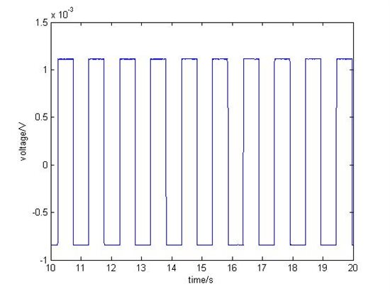
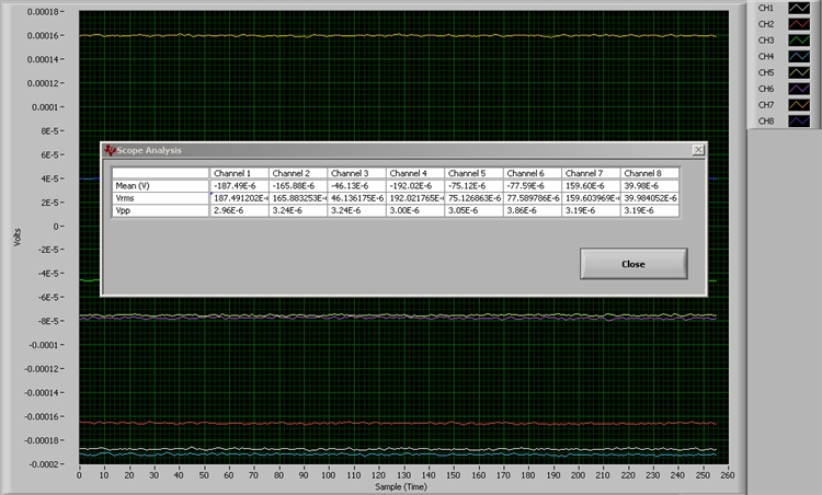
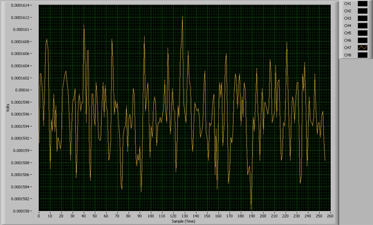
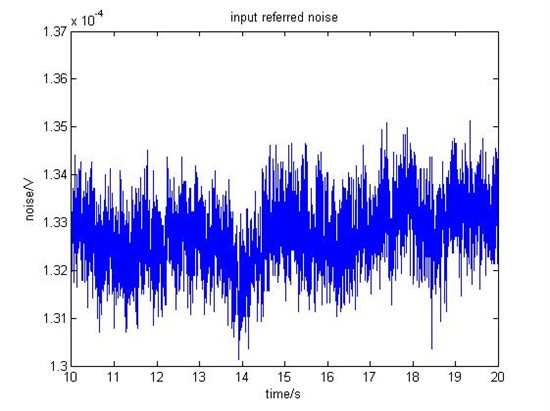
I got a problem with the input-referred noise.It is said on the datasheet that the peak to peak noise of ADS1298 is 3.5uV when analog supply=3V,reference volt=2.4V,output data rate=500sps,PGA gain=6 and the device is in the high resolution mode.But when i  follow the procedure written in page 78 of the datasheet to check the input referred noise using a circuitry designed by myself,it seems that the noise is about 130uV.This is the plot of noise.I don't know what is wrong. 

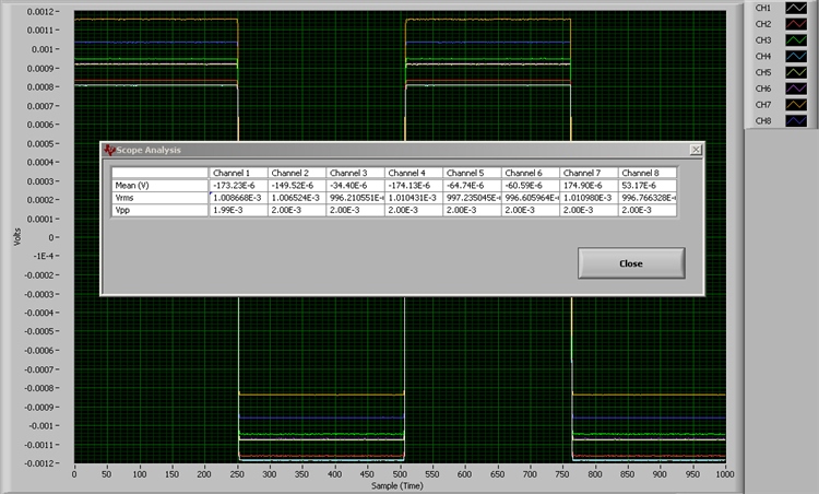
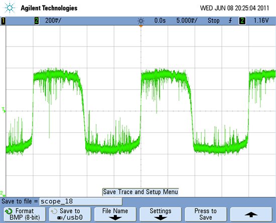
i also upload the plot of the 1mV internal test signal.

  • **TI EDIT February 20th 2019; FOR GENERAL ADS129x ASSISTANCE, PLEASE SEE NEW BIOPOTENTIAL FAQ LOCATED HERE**

    Hi bowen jing,

    Thank you for sharing your ADS1298 data with us!  The input referred noise is uVpp, so you should not include the DC offset.  Looking at your first plot, it seems you have something on the order of 5uVpp.  Below are a couple screen captures from our software.  First is all eight channels, second is CH7 by itself.

    The test signal (again ignoring offset) looks to be about 2mVpp.  I actually see similar results, when the TEST_AMP bit is cleared, I see 2mVpp and when set the amplitude looks to be 4mVpp - both are twice the value noted in the register tables so I'll look into that a little more.  Some additional screen shots for you showing the test signal - first all eight channels followed again by CH7 alone.


  • Hi,Tom

             Thank you so much. I shoudn't have include the DC offset.But the noise i got from my circuitry seems to be a little bigger than yours.I will check my circuitry again and see whether i can do some improvement about it. 

    Greetings from distant China !
  • Your noise does not look all that bad actually considering the amount of data you have gathered.  Note that the specification on page 4 for 10 seconds of data is typically 5uVpp, which is about what I saw in your graph. 

    A year ago today I was landing in Shanghai...

  • Oh!I see,i see.Your reply is quite helpful to me.Thank you very very much.

  • Hi Bowen Jing

    I am struggling to communicate with ADS1298 properly.

    I am using the on board MSP430F2274 from ez430-RF2500 to collect data from ADS1298, currently I have no circuity for the ADS1298 but simply power supply and digital connections.

    When I asked for data from ADS1298, it gave me random waveform, and I think it has nothing to do with noise, and of course can't be any circuit error, so perhaps the way I issued the commands was wrong.

    Would you mind to share your work to me so I can get through this please? as I have stuck in here for 3 months time.


    Thanks in advance.

  • The test signals are +/- so the 2mV and 4mV levels are normal.

  • Hi Weng Kou Chan

    I am really willing to share my work with you.But the problem is that i am using a LPC2210(ARM processor manufactured by philips) rather than MSP430 to communicate with ADS1298. Based on the mistakes i've made before i get the data correct,i suggest you pay attention to the SPI clock, the CS pin and internal reference. if you will ,please reply me with your e-mail address so that i can send you my programme code.Before i send the code to you,i have to translate the annotation from chinese to english and maybe you have to wait for several days because i am busy preparing to get my bachelor degree.

    greeting from distant CHINA

  • Hi Bowen Jing

    I appreciate for your generous help, I would like to use your code as an example perhaps to correct my code, thus the difference between MSP430 and LPC2210 should have no effect.

    I set the data rate of  ADS1298 to be 1000SPS, the SPL clock to be 1MHz, and the MPS430 should be running at speed of 16MHz. My current problem is reading the data from ADS1298. I was trying to read its ID version number, however DRDY and Data Output are both random signal, so I think there is a problem with my code, especially the timing between my instructions. 

    If you think you do have some spare time and is able to help me somehow, please visit this link 

    http://e2e.ti.com/support/data_converters/precision_data_converters/f/73/p/113513/408862.aspx#408862

    as I have some evidences from oscilloscope showing the timing requirement I achieved. Thanks in advance.

    Regarding the Chinese you use in your code, I am able to read it, as I am a Chinese as well, so the only matter is whether my computer can display them using the correct language, but again since I am chinese, I have chinese font and language installed, so should have no problem.

    Once again thanks for your generosity and good luck with your degree

    Here is my email address wkvictorchan@gmail.com

  • Thank you Bowen Jing, I have just received your email with the attachments.

    I forget to ask you a question, why did you advice me to pay attention of the internal reference please? what does it do and what is the importance of it? May I observe this 2.4V somehow on the chip?

    (I think I should ask you here rather than privately in email as here is still the forum to share questions and knowledges)

  • Hi Wen Kou Chan

    I have send my code with chinese annotation to your e-mail.The first one is for reading the ID.The second one is for testing the chip with internal test signal.Good luck!! 

  • Hi

    I once  made some silly mistake that i forgot to power on the internal reference and alway got some incorrect data output. But when you read the ID,it doesn't matter whether you are using the internal reference or external one.The internal reference only matters when you are using the ADC to digitalize input signal. You can check the datasheet for some further information about the reference voltage.Good luck.

  • Hi 

    I have just finished digesting your code, once again thank you for the help.

    I would like to confirm the procedure for conducting the noise test like what you have done. I have configured the registers according, I input NOTHING to the chip as the test signal is generated internally, I observe the result at pin TEST_PACE_OUT2, as I am using channel 1 and it is output at PACE_OUT2 by default. 

    Am I right please?

    Because this is what I observed at pin TEST_PACE_OUT2, I just don think it is correct at all. With the setting you have, I expect the signal have freq = 2.048MHz/ 2^21 = 0.9765Hz, but the signal below has frequency 50Hz, is it because I am powering it using a power supply plugged into main socket?

  • Hi 

    I wonder whether I am actually see that VREF (2.4V) at VREFP pin please? Because I set it to use internal reference, and all I see at VREFP is noise, not even a noise at a 2.4V DC level

  • Hi

    According to the "Test Signals (TestP and TestN)"subsection of "INPUT MULTIPLEXER"section,i am afraid you have to use TEST_PACE_OUT1  and TEST_PACE_OUT2 to monitor the internal test signal rather than only use TEST_PACE_OUT2. The default value of PACE Detect Register doesn't mean that you can observe the internal test signal only using TEST_PACE_OUT2 pin.The register seems only take effect when you use the PACE detection function in hardware approach.

  • So how exactly did you do perform the test signal measurement? in terms of the hardware procedure please.

  • Hi Victor

    Actually i didn't.I just feed the input with test signal, get the data output from the ADC, upload the data to the computer and then plot the data in the matlab which you have seen above.

  • Hi Bowen Jing

    You know in CONFIG2, there are TEST_AMP and TEST_FREQ that can be set, so you didn't obverse the pulse at fCLK/2^21 or fCLK/2^20?

    Again, am I able to see the internal reference 2.4V/4V somehow please?

  • NO,I didn't.As you see above,my plot have show you the frequence of the square waveform.

    About the reference,i advice you to ask Tom,as i didn't have my circiutry at hand and i am not able to do any measurement these days.So i don'know whether you can see the internal reference   

  • Hi Tom, How Are you? I have a question, I've created my own board, and I test the noise using the option input shorted, and i have a signal with 26uV of amplitude.Just considering the signal not the dc offset.


    How can I reduce that noise with hardware techniques.

    With that noise i am going to have some trouble with adc converter?

  • Hi, I have a question How can i know the internal operation of the device to know the offset system? I read the datasheet and doaesnt appear any information about that, how the device can measure the offset, I know if you configure the input channel as input shorted I'm going to see the offset, but internally how the device can measure the offset.

  • HI Tom,

    I've been trying to get de test signal from ADS1298 but I could not even, can you show me what is the correct register configuration to do that, the signal that I obtain is noisy and does not have a square form.

    I hope you help me!

    regards