This thread has been locked.

If you have a related question, please click the "Ask a related question" button in the top right corner. The newly created question will be automatically linked to this question.

ADS1293: ADS1293 12 Lead Experiment problem with Channel 1 data of 2nd and 3rd ADS1293

Part Number: ADS1293

Dear Friends,

I am trying to implement a 12-lead ECG reading circuit which is mentioned in the ADS1293 datasheet. (refer to datasheet Page No. 67).

https://www.ti.com/lit/ds/symlink/ads1293.pdf?ts=1665472582670&ref_url=https%253A%252F%252Fwww.ti.com.cn%252Fproduct%252Fcn%252FADS1293

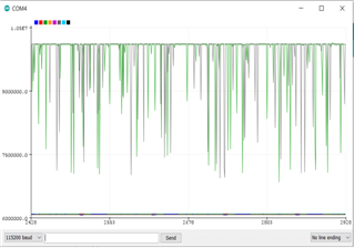
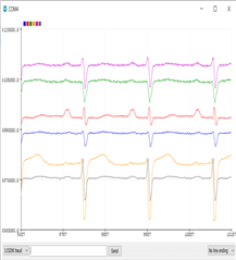
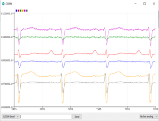
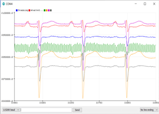
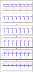
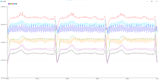
I am able to read Lead 1 and Lead 2 signals as well as the signals provided by Channel 2 and Channel 3 of the 2nd and 3rd ADS of the circuit. However, I cannot read the signal properly from the 1st channel of both the 2nd and 3rd ADS. Out of 12 Leads, I am able to properly read 10 signals and I am finding only noise in the remaining 2 signals.

The circuit implemented is precisely similar to the one provided in the datasheet. Can anyone help me in understanding where things are wrong? Thanks in advance for the help.

  • Hi,

    Let me understand and restate your question - "cannot read the signal properly from the 1st channel of both the 2nd and 3rd ADS."

    Do you use an ECG simulator?

    Dose that mean V1-WCT  and V4-WCT leads?  Are the ECG simulator's V nodes working properly, especially those nodes you think it's not proper? 

    If yes, have your tried place the V1 and V2 electrodes/patches to different nodes Vx?

    Do you try any different gain settings?

    When you say not properly, could you provide any screenshot or plot to show what does that mean?

    May I ask how did you deduce/debug to come to this observation that it's the 1st channel of both the 2nd and 3rd ADS not properly?

    Have you tried the internal test signal on those 1st channel of both the 2nd and 3rd ADS? and see how it comes out?

    Thanks

  • Dear Yang,

    Thank you for your reply. Apologies for the lack of clarity in my question.

    Yes the leads V1-WCT and V4-WCT leads are problematic and we are using WhaleTec MECG Simulator. We did try placing the electrodes on different nodes and we are getting the same kind of results. I will attach the results of the same and share them with you for further clarity.

  • Dear Yang,

    I have tried some simulations and tests and I am attaching the output of the same here.

    I selected an ECG wave on the simulator and I am attaching the outputs that I have obtained with respect to the signal. I am able to plot the signals properly only when I suppress the output from channel 1 of 2nd and 3rd ADS IC.

    Plot1. (Output with all the signals plotted together)

    Plot 2 Output of all the leads except V1 and V2

    Plot 3 Output when v1 swapped with v2 and v4 swapped with v5 on the ECG simulator


    Legends :

    Blue - Lead1; Red - Lead 2; Green- V2; Yellow - V3; Pink- V5; Grey- V6

    Original Signal From ECG Simulator :  Leads from the beginning V1, V2, V3, V4, V5 and V6.

    Observation: Channels 2 is able to show a proper signal even when the flex-register values of Channel 1 and Channel2 are swapped. However, there is some added noise being observed in that test on channel 2 signals. When physically swapped on the simulator, Channel 2 shows a valid signal which is fed to the Channel1.

    The error registers of each ADS were also noted and the corresponding values are as follows:

    ADS 1:

    ADS 2:

    ADS 3:

    Lead Off Detect Error  (0x18)

    0x00

    0x00

    0x00

    Error Status                   (0x19)

    0x00

    0x10

    0x10

    Error Range1                 (0x1A)

    0x34

    0x40

    0x40

    Error Range2                 (0x1B)

    0x34

    0x14

    0x14

    Error Range3                 (0x1C)

    0x00

    0x00

    0x00

    Error Sync                      (0x1D)

    0x00

    0x00

    0x00

    Error Misc                      (0x1E)

    0x03

    0x02

    0x02

    Please let me know of any other information you may need. Thanks for your help in advance.

  • Hi,

    I do not see output or screenshot.

    When you say not properly, could you provide any screenshot or plot to show what does that mean?

    Do you try any different gain settings?

    May I ask how did you deduce/debug to come to this observation that it's the 1st channel of both the 2nd and 3rd ADS not properly?

    And, just to confirm, the ECG simulator can output V1 and V4 correctly, right?

    Would you please clarify a bit more when you say  "Yes the leads V1-WCT and V4-WCT leads are problematic and we are using WhaleTec MECG Simulator. We did try placing the electrodes on different nodes and we are getting the same kind of results."

    What if you connect the V1 and V4 from ECG simulator to other input pins, the known good channel? How are the results&outcomes? 

    Do you know some Vx leads signals could be very small? Do you try increase the ECG simulator's amplitude if there is this option?

    Have you tried the internal test signal on those 1st channel of both the 2nd and 3rd ADS? and see how it comes out?

    Thanks.

  • Dear Yang,

     Apologies. I was not able to add the plots earlier and I have added them for your perusal. Please let me know if you need anything else.

  • Hi,

    Appreciate for the plots. It's suggested to tackle/solve problem/issue one by one and one at a time.

     Let's start with this "cannot read the signal properly from the 1st channel of both the 2nd and 3rd ADS."

    Could you try using a known good ECG simulator and inject a known good signal only to the 1st channel of the 2nd and 3rd ADS, one at a time, and see how the outcome are?

    Could you also try configure the 1st channel of the 2nd and 3rd ADS to internal test signals, read/acquire one at a time, and see how the outcome are?

    One more question, what do you mean by "suppress the output from 1st channel of the 2nd and 3rd ADS"?


    Thanks

  • Thank you Cheng for your reply. Apologies for the delay in my response. Let me reply to it in the order.

    Could you try using a known good ECG simulator and inject a known good signal only to the 1st channel of the 2nd and 3rd ADS, one at a time, and see how the outcome are?

    We are WhaleTeq's MECG 2000  ECG simulator and we are injecting a proper known signals only. But as per your suggestion we are yet to try out injecting signal only in the 1st Channel of 2nd and 3rd ADS. We will be sharing the plots with you as soon as we get it. Just to clarify, I would still have to apply the limb lead signals to the Ist ADS to obtain the Wilson's Central Terminal section for the chest leads to be measured. I will only be removing the V2, V3 and V5, V6 signals from the board.

    Could you also try configure the 1st channel of the 2nd and 3rd ADS to internal test signals, read/acquire one at a time, and see how the outcome are?

    We will be trying that and sending you the plots. We have tried working with the test signals before but we could not understand if we were getting proper plots and hence, we have stopped working on it for a while. If it is possible can you please share us the register configurations that we will have to use in order to try and obtain the test signals? Thank you.

    One more question, what do you mean by "suppress the output from 1st channel of the 2nd and 3rd ADS"?

    By "suppress the output", I mean commenting out the values from the code so that they are excluded from the plot. I had written the code to plot all the outputs as I get them and it was observed that it is difficult to see the response of the other signals as the plotter adjusts itself to allocate the signals in the view. Proper outputs are only seen if the Channel 1 output of 2nd and 3rd ADS are not included in the plotting.

    Let me know if you would need anything more. We will get back with the plots asap.

    Thank you.

  • Hi,

    Thanks for the reply.

    some more comments, please turn off/disable any LEAD OFF and PACE detection.

    And, please also try the internal test signals.

  • Hello Yang,

    I would like to inform you that after trying to disable the Lead Off and Pace detection, I found that many register values which were not assigned in the setting up process where getting assigned garbage values. As a result, in IC 2 and IC3, Pace detection register (0x04) was not having 0x00 which was expected. Also, the high output that was being observed in the channel1 output of IC2 and IC3. Then the AFE_shutdown_reg (0x14) was seen to be shutting down the Instrumentation Amplifier connected to channel 1 in IC2 and IC3. This was the reason due to which the IC2 and IC3 channel 1 was not at all affected even if there was a signal applied or not. When the instrumentation amplifier was enabled on channel 1, we were able to see the data on Channel 1 of IC2 and IC3. We have applied the relevant changes in the respective setup routines. I am attaching the screenshots in which all the eight signals (I,II,V1 to V6) are properly recorded in the serial monitor.

    We thank you for the support you have been providing till now. We would also like to remind you that the root cause for the problem was the IC's registers not defaulting to their respective default values. Perhaps this same issue may be occurring in other ADS1293 ICs.

    Thank you and have a nice day.

  • Hi 

    Really appreciate for letting me know.

    Good lesson learned for me - "always RESET and double check the initialization processes."

  • Which controller and ADS1293 development board are you using?

  • Hi Kushal,

    Are you asking me or to the customer?

    TI has ADS1293 development board(EVM) -

    www.ti.com/.../ADS1293EVM

    and it uses MSP430F5529IPN MCU.

    I cannot and not allowed to answer for other customers.

    Thanks

  • We are not using any development board. We have used ADS1293 ICs itself. The circuit we have made is given in the ADS1293 datasheet. You can use any controller with it as the ADS1293 uses SPI to communicate.

  •  

    Actually we are using esp32 with ADS 1293 development board from protocentral. With same development board we are able to get ECG waveform with arduino. But when we are using ESP32, we are not getting proper output. I have tested out SPI communication. It is able to read and write data into registers.

    can you help out in this?

  • Also, As I can see from the above posts, I can see arduino IDE. which microcontroller are you using?

  • Can you check the values of OSC Control Registers (0x12) and AFE Control registers (0x13, 0x14 and 0x15)? Apparently sometimes, the registers do not go back to default values when not assigned. Make a list of all the registers that you are not assigning in your program and double check their values by reading them.

    Also, How is your output? Are you having a constant zero output? Something very noisy or Just inaccurate signal?

  • Hi

    I have checked values and it is as follows:

    0x12 =4

    0x13= 0

    0x14=36

    0x15=0

    Also I got following output.

  • Also, Here is the code i am using.

    //#include <SPI.h>
    
    /*
    
      Simplest 3-Lead 24-bit ECG with an ads1293 and esp32
    
      SPI conection:
    
      ads1293     Esp32 Pico
      DRDYB       D4
      SDO         D12 (slave out - master in )
      SDI         D13 (slave in  - master out)
      SCLK        D14
      CSB         D15
      ALARMB      D2
    
    */
    
    // #include "Plotter.h"
    // Plotter p;
    
    #include <SPI.h>
    
    SPIClass * vspi = NULL;
    //SPIClass vspi(VSPI);
    static const int spiClk = 1000000; // 1 MHz
    
    const int pin_DRDYB = 4;  // data ready
    const int pin_ALARMB = 2; // alarm
    const int pin_MISO = 19;  // MISO
    const int pin_MOSI = 23;  // MOSI
    const int pin_SCLK = 18;  // SCLK
    const int pin_SS = 5;    // CSB
    
    int32_t c1;
    int32_t c2;
    int32_t c3;
    
    double cd1;
    double cd2;
    double cd3;
    
    int32_t getValFromChannel(int channel)
    {
      byte x1;
      byte x2;
      byte x3;
    
      switch (channel)
      {
      case 1:
        x1 = 0x37;
        x2 = 0x38;
        x3 = 0x39;
        break;
      case 2:
        x1 = 0x3A;
        x2 = 0x3B;
        x3 = 0x3C;
        break;
      case 3:
        x1 = 0x3D;
        x2 = 0x3E;
        x3 = 0x3F;
        break;
      }
      int32_t val;
    
      // 3 8-bit registers combination on a 24 bit number
      val = readRegister(x1);
      //Serial.println(readRegister(x1));
      val = (val << 8) | readRegister(x2);
      //Serial.println(readRegister(x2));
      val = (val << 8) | readRegister(x3);
      //Serial.println(readRegister(x3));
      
     // delay(1000);
      //val = val << 8;
      //val = (int32_t) (val);
    
      return val;
    }
    
    void setup_ECG_2_channel()
    {
      // datasheet ads1293
      //Follow the next steps to configure the device for this example, starting from default registers values.
      //1. Set address 0x01 = 0x11: Connect channel 1’s INP to IN2 and INN to IN1.
      writeRegister(0x01, 0x11);
      //2. Set address 0x02 = 0x19: Connect channel 2’s INP to IN3 and INN to IN1.
      writeRegister(0x02, 0x19);
      //3. Set address 0x0A = 0x07: Enable the common-mode detector on input pins IN1, IN2 and IN3.
      writeRegister(0x05, 0x00);
    
      
      writeRegister(0x0A, 0x07);
      //4. Set address 0x0C = 0x04: Connect the output of the RLD amplifier internally to pin IN4.
      writeRegister(0x0C, 0x04);
      //5. Set address 0x12 = 0x04: Use external crystal and feed the internal oscillator's output to the digital.
      writeRegister(0x12, 0x04);
      //6. Set address 0x14 = 0x24: Shuts down unused channel 3’s signal path.
      writeRegister(0x14, 0x24);
      //7. Set address 0x21 = 0x02: Configures the R2 decimation rate as 5 for all channels.
      writeRegister(0x21, 0x02);
      //8. Set address 0x22 = 0x02: Configures the R3 decimation rate as 6 for channel 1.
      writeRegister(0x22, 0x02);
      //9. Set address 0x23 = 0x02: Configures the R3 decimation rate as 6 for channel 2.
      writeRegister(0x23, 0x02);
      //10. Set address 0x27 = 0x08: Configures the DRDYB source to channel 1 ECG (or fastest channel).
      writeRegister(0x27, 0x08);
      //11. Set address 0x2F = 0x30: Enables channel 1 ECG and channel 2 ECG for loop read-back mode.
      writeRegister(0x2F, 0x30);
      //12. Set address 0x00 = 0x01: Starts data conversion.
      writeRegister(0x00, 0x01);
    }
    
    void setup_ECG_3_channel()
    {
      // datasheet ads1293
      //Follow the next steps to configure the device for this example, starting from default registers values.
      //1. Set address 0x01 = 0x11: Connect channel 1’s INP to IN2 and INN to IN1.
      writeRegister(0x01, 0x11);
      //2. Set address 0x02 = 0x19: Connect channel 2’s INP to IN3 and INN to IN1.
      writeRegister(0x02, 0x19);
    
      writeRegister(0x03, 0x2E); //diff
    
      //3. Set address 0x0A = 0x07: Enable the common-mode detector on input pins IN1, IN2 and IN3.
      writeRegister(0x0A, 0x07);
      //4. Set address 0x0C = 0x04: Connect the output of the RLD amplifier internally to pin IN4.
      writeRegister(0x0C, 0x04);
    
      writeRegister(0x0D, 0x01); //diff
      writeRegister(0x0E, 0x02); //diff
      writeRegister(0x0F, 0x03); //diff
    
      writeRegister(0x10, 0x01); //diff
    
      //5. Set address 0x12 = 0x04: Use external crystal and feed the internal oscillator's output to the digital.
      writeRegister(0x12, 0x04);
      // //6. Set address 0x14 = 0x24: Shuts down unused channel 3’s signal path.
      // writeRegister(0x14, 0x24);
      //7. Set address 0x21 = 0x02: Configures the R2 decimation rate as 5 for all channels.
      writeRegister(0x21, 0x02);
      //8. Set address 0x22 = 0x02: Configures the R3 decimation rate as 6 for channel 1.
      writeRegister(0x22, 0x02);
      //9. Set address 0x23 = 0x02: Configures the R3 decimation rate as 6 for channel 2.
      writeRegister(0x23, 0x02);
    
      writeRegister(0x24, 0x02); //diff
    
      //10. Set address 0x27 = 0x08: Configures the DRDYB source to channel 1 ECG (or fastest channel).
      writeRegister(0x27, 0x08);
      //11. Set address 0x2F = 0x30: Enables channel 1 ECG and channel 2 ECG for loop read-back mode.
      writeRegister(0x2F, 0x70); //diff
      //12. Set address 0x00 = 0x01: Starts data conversion.
      writeRegister(0x00, 0x01);
    }
    
    //===========SPECIALIZED SPI OPTION 1
    byte readRegister(byte reg)
    {
      byte data;
      reg |= 1 << 7;
      vspi->beginTransaction(SPISettings(spiClk, MSBFIRST, SPI_MODE0));
      digitalWrite(vspi->pinSS(), LOW);
      vspi->transfer(reg);
      data = vspi->transfer(0);
      digitalWrite(vspi->pinSS(), HIGH);
      vspi->endTransaction();
      return data;
    }
    
    void writeRegister(byte reg, byte data)
    {
      reg &= ~(1 << 7);
      vspi->beginTransaction(SPISettings(spiClk, MSBFIRST, SPI_MODE0));
      digitalWrite(vspi->pinSS(), LOW);
      vspi->transfer(reg);
      vspi->transfer(data);
      digitalWrite(vspi->pinSS(), HIGH);
      vspi->endTransaction();
    }
    //===========SPECIALIZED SPI
    
    void setup()
    {
    
      vspi = new SPIClass(VSPI);
      vspi->begin();
      //vspi->begin(pin_SCLK, pin_MISO, pin_MOSI, pin_SS);
      pinMode(pin_DRDYB, INPUT);
      pinMode(pin_ALARMB, INPUT);
      pinMode(pin_SS, OUTPUT);
      pinMode(vspi->pinSS(), OUTPUT);
    
      Serial.begin(115200);
      
      //SPI.begin();
     // Wire.begin(25,22);
      //vspi->setClockDivider (SPI_CLOCK_DIV16);
      //vspi->setBitOrder (MSBFIRST);
      //vspi->setDataMode (SPI_MODE0);
      //option 1: use vspi specific spi channel
      //vspi.begin(pin_SCLK, pin_MISO, pin_MOSI, pin_SS);
    
      //option 2: use default spi class methods
      //SPI.begin(pin_SCLK, pin_MISO, pin_MOSI, pin_SS);
    
      setup_ECG_2_channel();
      int i = 0x00;
      while(i <= 0x3F)
      {
        Serial.println(i);
        Serial.println(readRegister(i));
        i++;
        
        
        }
    //  Serial.println(readRegister(0x01));
    //  Serial.println(readRegister(0x02));
    //  Serial.println(readRegister(0x03));
    //  Serial.println(readRegister(0x04));
    //  Serial.println(readRegister(0x05));
    //  Serial.println(readRegister(0x06));
    //  Serial.println(readRegister(0x07));
    //  Serial.println(readRegister(0x08));
    //  Serial.println(readRegister(0x09));
    //  Serial.println(readRegister(0x0A));
    //  Serial.println(readRegister(0x0B));
    //  Serial.println(readRegister(0x0C));
    //  Serial.println(readRegister(0x0D));
    //  Serial.println(readRegister(0x0E));
    //  Serial.println(readRegister(0x0F));
    //  Serial.println(readRegister(0x10));
    //  Serial.println(readRegister(0x11));
    //  Serial.println(readRegister(0x12));
    //  Serial.println(readRegister(0x13));
    //  Serial.println(readRegister(0x14));
    //  Serial.println(readRegister(0x15));
    //  Serial.println(readRegister(0x16));
    //  Serial.println(readRegister(0x17));
    //  Serial.println(readRegister(0x18));
    //  Serial.println(readRegister(0x19));
    //  Serial.println(readRegister(0x1A));
    //  Serial.println(readRegister(0x1B));
    //  Serial.println(readRegister(0x1C));
    //  Serial.println(readRegister(0x1D));
    //  Serial.println(readRegister(0x1E));
    //  Serial.println(readRegister(0x1F));
    //  Serial.println(readRegister(0x20));
    //  Serial.println(readRegister(0x21));
    //  Serial.println(readRegister(0x22));
    //  Serial.println(readRegister(0x23));
    //  Serial.println(readRegister(0x24));
    //  Serial.println(readRegister(0x25));
    //  Serial.println(readRegister(0x26));
    //  Serial.println(readRegister(0x27));
    //  Serial.println(readRegister(0x28));
    //  Serial.println(readRegister(0x29));
    //  Serial.println(readRegister(0x2A));
    //  Serial.println(readRegister(0x2B));
    //  Serial.println(readRegister(0x2C));
    //  Serial.println(readRegister(0x2D));
    //  Serial.println(readRegister(0x2E));
    //  Serial.println(readRegister(0x2F));
    //  Serial.println(readRegister(0x30));
    //  Serial.println(readRegister(0x31));
    //  Serial.println(readRegister(0x32));
    //  Serial.println(readRegister(0x33));
    //  Serial.println(readRegister(0x34));
    //  Serial.println(readRegister(0x35));
    //  Serial.println(readRegister(0x36));
    //  Serial.println(readRegister(0x37));
    //  Serial.println(readRegister(0x38));
    //  Serial.println(readRegister(0x39));
    //  Serial.println(readRegister(0x3A));
    //  Serial.println(readRegister(0x3B));
    //  Serial.println(readRegister(0x3C));
    //  Serial.println(readRegister(0x3D));
    //  Serial.println(readRegister(0x3E));
    //  Serial.println(readRegister(0x3F));
    //  Serial.println(readRegister(0x40));
    //  Serial.println(readRegister(0x50));
      delay(1000000);
      //setup_ECG_2_channel();
    
      // p.Begin();
      // p.AddTimeGraph("3 channel graph", 1000, "c1 label", cd1, "c2 label", cd2, "c3 label", cd3);
    }
    
    void loop()
    {
      // if (digitalRead(pin_ALARMB) == false)
      // {
      //   Serial.println("alarm raised");
      // }
      if (digitalRead(pin_DRDYB) == false)
       {
    
      // sampled data is located at 3 8-bit
      //--CHANNEL 1
      c1 = getValFromChannel(1);
      // cd1 = (double)c1;
      Serial.print(c1);
    
      Serial.print(",");
      //--CHANNEL 2
      c2 = getValFromChannel(2);
      // cd2 = (double)c2;
      Serial.print(c2);
    
      Serial.print(",");
      //--CHANNEL 3
      c3 = getValFromChannel(3);
      // cd3 = (double)c3;
      Serial.println(c3);
    
      // p.Plot();
       }
      delay(100); //20ms delay
    }

  • Thanks for the discussion here.

    I will keep this thread Open.

    Thanks