This thread has been locked.
If you have a related question, please click the "Ask a related question" button in the top right corner. The newly created question will be automatically linked to this question.
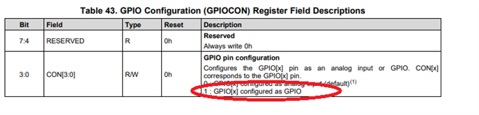
Is lt possible to configure GPIO pins (GPIO_0/Ain1, Gpio_1,GPIO_2, GPIO_3 asdigital inpuut/output pins. That seems to be the case per the manual.
However, when I try to configure the port as follows
WREG 11 00 // configure port pins as outputs
WREG 10 0F // set output high
The pins are not changing - staying low. I expected them to go high and low depending what I write to lower 4 bits setting in the WREG 0x, where x is the value.
The GPIo pins are not changing. Waht am i doing wrong?
When I press the sync button and the write to register button, The system indicates that it wrote to tthe device.
Hi Napoleon,
Welcome to the E2E forum! I refer you to Table 43 in the ADS114S08 datasheet.
Note that for register 0x11, the bit settings should be set to '1' to make the pin set to GPIO mode. So the correct register setting would be WREG 11 0F to make the pin as a GPIO. Register 0x10 then sets the action of the GPIO as Input or Output (upper 4 bits) with the lower four bits as value on the pins. So the register 0x10 setting appears correct for your use case. When register 0x10 is set to Input mode (upper 4 bits high) then when you issue a register read for register 0x10, the lower four bits will indicate the value at the pin.
You can mix and match the combinations as well, but writing to an Input pin will have no effect.
Best regards,
Bob B
Bob,
Thanks! You are right. I provided the wrong information. I did attempt WREG 11 0F followed by WREG 10 0F, I was not able to affect the state of the pins. Under the Sigma Delta Evaluation software Console , those pins were configured as output or input and the corresponding GPIOxdata was set to high or low. The GPIO pins did not change and stayed low. I did click on the "write Selected Register", "Refresh/Sync",
Hi Napoleon,
I'm not sure why initially you had issues, but glad to hear you were able to succeed.
I also tried it on the EVM and verified it does work. There is one thing to note with respect to the EVM however. The EVM is designed to use the pins as analog inputs. You may see a lower than expected voltage due to the input filters. Also for GPIO2 (AIN10) and GPIO3 (AIN11) there is a jumper (JP13) that should be removed as the jumper terminates the input to either AGND or VREF which will affect the voltage read at the terminal blocks. Please see the schematic in the user's guide to follow the current output path from the pin.
Best regards,
Bob B
The truth is that I am somewhat puzzled ,as well. I will investigate that later on. I was only using ain8 & 9 for testing purposes. Thanks for pointing out J13, though.