This thread has been locked.

If you have a related question, please click the "Ask a related question" button in the top right corner. The newly created question will be automatically linked to this question.

ADS1234: Connect ADS1234 using SPI

Part Number: ADS1234
Other Parts Discussed in Thread: ADS1232

Hi guys !

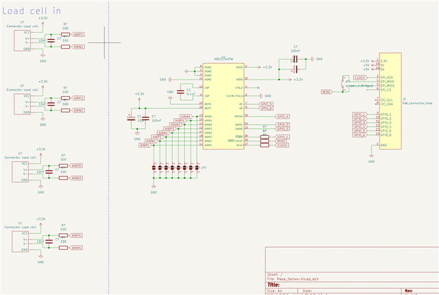
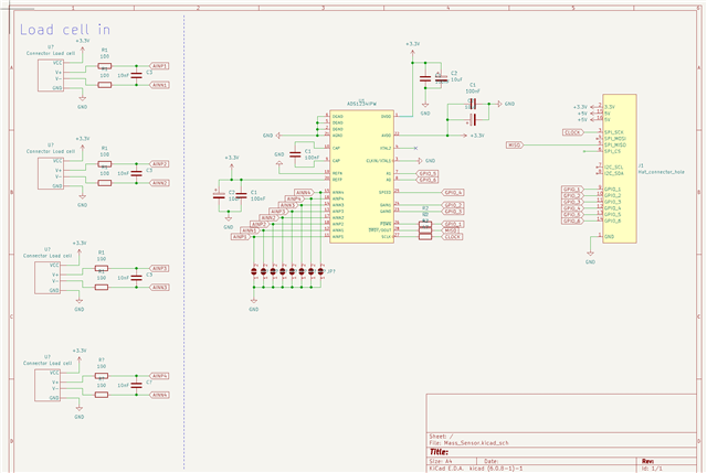
I am studying electrical engineering in second year and for a university project I want to connect 4 loads cells to the main board. Since I want 4 inputs, I decide to use ADS1234. The ADC seems to be compatible with SPI but, as far as I understand the point of SPI, the name of the pins of the ADS1234 are note the sam as "normal SPI's pin" and I don't really know how to connect the ADC. I try this but I don't know if it is correct...

Here is my schematic for the moment, do not hesitate if you have any advice or modifications !!

Thanks a lot.

Sorry for my English

  • Other question : Can I connect the ADC with I2C ?

  • Hi Tomas,

    Welcome to the E2E forum!  Let me answer your last question first.  No, you cannot connect the ADS1234 to I2C as there is no response mechanism within the ADS1234 to ACK communication as there is no communication input pin that is bidirectional.  

    The way you show the digital connections is mostly correct, although there should not be a jumper connection between MISO and MOSI.  To initiate a conversion read you normally would write dummy contents to the TX register/buffer (even though the MOSI is not connected) to start initiating the SCLKs.

    I would suggest using a common ground and that the ground be a solid plane (not just trace connections).  AGND and DGND must be at the same level.  If you do split the grounds, then where the grounds join together do not use ferrites or inductors in the connection between the two.

    You should also have a 100nF bypass/decoupling cap at the DVDD pin of the ADS1232.

    The capacitor near the load cell connectors should be on the other side of the resistors to provide a low-pass filter.  In other words the capacitor should be between the resistors and the ADC input pins.

    You may find A Basic Guide to Bridge Measurements a useful resource.

    Best regards,

    Bob B

  • Hello,

    thanks, you are helping me a lot ! This is my first design of PCB...

    Here is the design with the modifications, do you have any advice or remarks, can I improve it or it should work like that ? Other question, is it really useful to  use both Cap and Polarized Cap ?

    Thanks !

    Tomas 

  • Hi Tomas,

    It is not always necessary to have the parallel caps for both decoupling and as a bulk charge reservoir.  But it wouldn't hurt for you to have the cap footprints and only populate if required.

    The schematic appears fine.  Your biggest concern is going to be noise pickup and issues with PCB layout.  Once you have created your PCB layout, zip to a file the gerber output files for me to review.

    Best regards,

    Bob B

  • Thanks a lot ! Is it normal to not connect the XTAL2 pin ?

    Can I improve the design to reduce the noise ?

  • Hi Tomas,

    The XTAL2 pin is used for when an external crystal is applied to create a clock source for the ADC.  When the CLKIN/XTAL1 pin is grounded the ADS1234 uses the internal oscillator as a clock source.  So in this case you would leave the XTAL2 pin floating.

    As far as noise, the bulk of your noise will most likely be picked up as EMI/RFI noise along the load cell cabling as the cable will act as an antenna.  There are a number of ways that the noise can be reduced such as using shielded cabling with the shield properly terminated to ground.

    When doing the PCB layout have a solid ground plane and make sure that the digital signals do not cross into the analog domain.  There are some good discussions in the TI Precision Labs on TI.com.  One topic is on NOISE and another on PCB layout.

    As far as circuit improvement, there are many possibilities, but the best way to learn is by building and testing your system.  Right now your schematic is showing a good start and should function as expected.  However after connecting your load cells you may find that there is room for further improvement.

    Best regards,

    Bob B