This thread has been locked.

If you have a related question, please click the "Ask a related question" button in the top right corner. The newly created question will be automatically linked to this question.

ADS114S08: What's the VOL (Logic output level) of GPIO_low when IOL = 10uA for ADS114S08 and ADS124S08's GPIO?

Part Number: ADS114S08
Other Parts Discussed in Thread: ADS124S08,

Hi team,

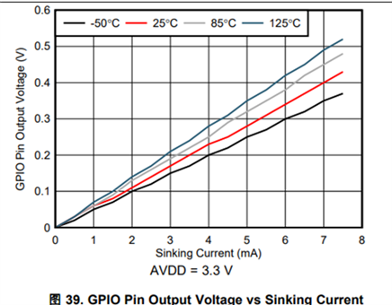
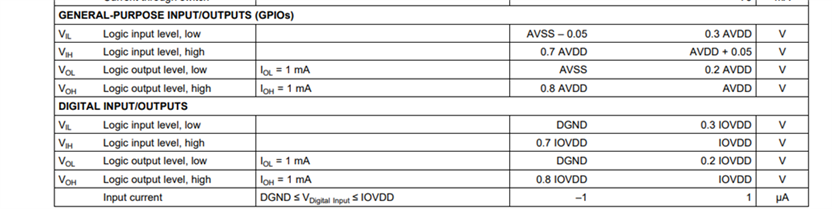
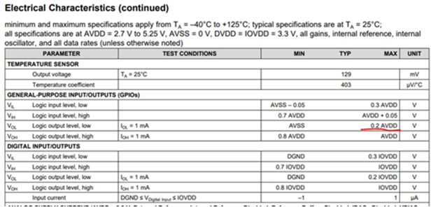
We use ADS114S08 and ADS124S08 to drive MOS, in the datasheet write" Vol MAX arrived at 0.2*AVDD, when IOL = 1mA".  But now our MOS Gate leakage current only have 10uA, Vth= 0.3~ 0.7V, we want to know what the maximum VoL at this time is. We must require MOS is turn off when GPIO is Low level. Please help to check whether it is feasible.

I'm looking forward to your reply soon!

Best regards, Hao

EC, FAE

  • Hi team,

    Sorry, I need to describe the problem more detail as follow: 

    We can see the Fig39 in ADS124S08 and ADS114S08, the Sinking current 1mA means GPIO output voltage below 0.1V, but in the Electrical Characteristics, we can see the Max GPIO Vol arrived at 0.2*AVDD=0.2*3.3=0.66V, which means IoL more than 8mA in the fig39.  

    See Fig 39, GPIO could connect MOS (Vth 0.3V) directly, but see Electrical Characteristics we couldn't connect it with MOOS directly. So how to understand Fig 39 and Electrical Characteristics? Which value is right? 


    I'm looking forward to your reply soon!

    Best regards, Hao

    EC, FAE

  • Hello Hao,

    Both the table and the graph are correct, but there may be some misunderstanding in interpreting what is being shown.  The electrical characteristics table is showing the device response for a specific condition.  The condition is with a 1mA loading at 25 deg C and these numbers are the guaranteed specifications for that operation. 

    Figure 39 graph is showing typical GPIO current over various temperature ranges and different current loading.  Figure 39 was added because many customers connect the GPIO to devices not specifically logic devices.  There is a desire to know and understand the behavior of the analog GPIO in higher than 1mA loading conditions.

    A complimentary MOS device (CMOS) has an active push-pull driver stage that when operating at a logic high turns on the PMOS device connected to the AVDD supply while the NMOS device is turned off.  A logic low turns off the PMOS device and turns on the NMOS device to AVSS.  In any case there will be some inherent resistance in the MOS devices.  The higher the current the greater the loading across the MOS resistances which will lower the logic high voltage and increase the logic low voltage.

    The outcome of the loading is shown in Figure 39 where when little current is being drawn, the logic low is close to 0 (AVSS is connected to AGND in this case) and when the loading is high the output voltage increases as the voltage drop across the NMOS resistance also increases.

    A standard CMOS device input will have only a small loading affect.  The result is the voltage for logic high is much closer to AVDD and logic low is much closer to AVSS.

    As to differences between the graphs and the table remember one is typical and the other is guaranteed.  There will be some lot to lot and device to device variation.  The MOS devices may vary some with respect to resistances when the MOS device is turned on.  The effect of the MOS resistance will depend on the current loading.

    Best regards,

    Bob B

  • Hi Bob,

    Thank you, Bob~

    Customers want to ensure information as follow: 

    Could we give the guaranteed value of GPIO_VOL when load current arrived at 10uA or below 10uA? Not only give the typical value like fig39.

    Best regards,

    Hao

  • Hi Hao,

    The guaranteed value is with the conditions specified in the datasheet.  There should be no need to further guarantee performance at less currents.  The reason for this is by basic circuit analysis.  Consider the GPIO as analog switches with some value of resistance associated with the RON value of the switch.  When turning on the low-side switch there is a path to AVSS (AGND with unipolar supplies).  We can calculate the worst case switch resistance for 3.3V AVDD as being Vol (max) divided by the 1mA current from the guaranteed specification value.  The result of ((3.3V * 0.2) / 1mA) is equal to 660 Ohms.

    If we now calculate for 10uA we see a voltage of 10uA * 660 Ohms which equals 6.6mV.  This is much closer to 0V and follows the graph in Figure 39.

    Best regards,

    Bob B