This thread has been locked.

If you have a related question, please click the "Ask a related question" button in the top right corner. The newly created question will be automatically linked to this question.

ADS8686SEVM-PDK: Not getting correct data in the channels using ADS8686s EVM - GUI

Part Number: ADS8686SEVM-PDK


Hello, 

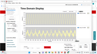
I have connected three different sensors to the three channels in ADS86867S EVM, in T3 block. I need to acquire the three sensors data simultaneously in the CSV file for every second. For this, I have set the following configuration in GUI. However, I am not getting the correct readings in the three channels output. Mostly three channels are displaying the same values. I am also getting the CSV files but all are same values. Kindly help me out to get the correct data from the three channels. In other words, How should I configure in GUI (in stack sequencer configuration, and device configuration) to get the three channels output in CSV.  Kindly help me out. 

In Board:

Sensor 1 - T3 (pin 1 and pin 2 for AIN7 + and AIN7_GND)

Sensor 2 - T3 (pin 3 and pin 4 for AIN6 + and AIN6_GND)

Sensor 3 - T3 (pin 5 and pin 6 for AIN5 + and AIN5_GND)

After this, In GUI, I have set the following configurations: 

Device configuration: 

Channel A Selection: Channel 7

Channel B Selection: Channel 0

Sampling rate target: 2kHz

Interface mode: Parallel, Device mode: Software, Sequencer mode: enabled, Burst Mode: Enabled

Sequencer Configuration: 

Stack1: Channel A Selection:  7                  Channel B Selection: 0

Stack2: Channel A Selection:  6                  Channel B Selection: 1

Stack3: Channel A Selection:  5                  Channel B Selection: 2

Last layer: Tick at Stack 3

  • I also need to know whether i have set the correct configuration for my requirement. I have read the datasheet. However, it is confusing. Please help me out to get the right configuration for my requirements. 

  • Hi Gopinath,

    I did not see any issue in your configuration. Can you upload a screenshot of the device configuration page in your GUI so that I can double check? Do you have any jumpers on the EVM? Please note that the EVM needs an external 5.5V power supply on T1 terminal.

    Best regards,

    Dale

  • Hello Dale, 

    Thanks for your reply. I have tested again. Currently, jumpers are placed on the JP6 and JP7 ( Placed on EXT and 5.5V). I have configured the settings for the three different sensors. The values at the T3 block terminal for the three sensors are showing different. However, the output values of the channels in the GUI is same for all the three channels. This is the problem I am facing. I could not resolve this. I have attached the screenshot and videos for your reference. 

    Kindly help me out to get correct values for the three channels.


  • Hi Gopinath,

    Thank you for providing more information. Your device configuration in the GUI is correct, I verified it on my EVM, it worked well. It seems like the sequencer on your device is not working. Did you install any other jumpers except J6 and J7 on your EVM? I can not see your board clearly. Is your EVM a new EVM? Did you do any modification on the EVM? Did you download the GUI from TI.com?

    Best regards,

    Dale

  • Hi Dale, 

    Thanks for your reply. No we did not install any other jumpers except J6 and J7. Further, the EVM is new and bought two months back only.

    We tried to use the EVM as a stand alone without PHI. For that we removed the R28 Zero ohm resister as mentioned in the Manual. However, It takes time to write the firmware and there is no open source library available. Therefore, We wanted to use this EVM with GUI for now. For this we again placed the R28 zero ohm resistor. 

    Yes, the GUI has been downloaded from the TI.com only.

    Kindly help us to resolve this issue.

  • Hi Gopinath,

    I will help you solve this issue. Can you please use a short wire to connect AIN7+ and AIN7_GND on T3 terminal? also please use another short wire to connect BIN0+ and BIN0_GND on T4 terminal, use the same configuration you did in device configuration in the GUI, then capture data. Please provide a screenshot of time domain so I can double check the result. 

    Thanks&regards,

    Dale

  • Hi Gopinath,

    When you insert a wire into the terminal T3 or T4, please make sure you insert the wire into the top side of terminal connector, please see my highlight in red.

    Best regards,

    Dale

  • Hi Dale, 

    thanks for your reply. I will get back to you after trying your suggestion. 

  • Okay. Noted Dale. 

  • Hi Dale, 

    We have tried this concept. However, the problem did not get solved. We are getting same values at the channels. I have attached the screenshots for your reference. 

  • Hi Gopinath,

    Thank you for your test. The burst sequencer mode on the ADC is working, however the conversion code/voltage (2.09V) shown in the GUI indicate that the ADC's input on 6 channels are floating, 2.09V is the default voltage for +/-10V input range when the ADC's input is floating, so I'm pretty sure this is a hardware connection issue. Can you please check the connection between the terminal block and the ADC's input? e.g. you have shorted pin 1 and 2 on T3 terminal block together with a wire which short AIN7 channel input on the ADC to GND, so 

    1. You should be able to get 0Ω on Q1 and 1kΩ on Q2 test point when you use your multimeter to measure the resistance between the test points and GND.
    2. You should be able to see 0V on Q1 and Q2 after your ADC board is powered up, and also should be able to see 0V conversion result on CH7A channel in the GUI software. If the voltage you measure on Q2 is 2.09V, your connection between the red wire on T3 terminal block and Q1/Q2 test point is open, you can specially check the wire connection on the T3 terminal block.

    Let me know the result once you check them, thanks.

    Best regards,

    Dale

  • Dear Dale, 

    Thanks for your suggestion. We have tried it. The following are our findings. 

    1) When the ADC is not powered up, we observed the resistance of 0.5 Ω (may be due to wire resistance) at Q1, and 1kΩ at Q2. 

    2) When the ADC is powered up, we observed the 0V at Q1 and Q2. But we got 2.10 V in Channel 7A in GUI. Further, we also observed  0V in Channel 4 and 5 on the Q1 and Q2 points. However, we observed 2V at Q1 and Q2 points of the Channel 6. 

    We hope there will be a solution to this issue from you. 

    Best Regards

    Gopinath 

  • Hi Gopinath,

    Thank you for your measurement.

    • How about the resistance between Q2 and the input pin (Ch-7A or Ch-4/5) on the ADC device when the ADC is not powered up?
    • When you measured 0V at Q2 point on the channels you mentioned (Ch-7A or Ch-4/5), what's the voltage on the analog input pin of the ADC device?

    If you measure 0ohm for my first question and 0V on the AINx pin of these channels, but got 2V or 2.1V in the GUI, your ADC device has been damaged, I would suggest you request a sample and replace the ADC device on the EVM board.

    Best regards,

    Dale

  • Dear Dale, 

    Thanks for your reply. We have found the following observations. 

    1) When the ADC is not powered up, the resistance between Q2 and the input pin (Ch-7A , 6A, 5A, and 4A) are 1k ohm. 

    2) The voltage on the analog input pin of the ADC is 5.5 V (I hope you have asked about the external analog power supply given to the EVM) 

    3) Further, we noted that for the configuration without sequencer enabled, we observed 0V on Q1, Q2 and also in the conversion result in GUI Ch 7A. We have attached the screenshot. 

    Another observation: 

    We connected two sensors to EVM. One sensor in the T2 terminal (Ch A0) and another sensor in T4 (Ch B0). With the configuration of channel A as Ch0 and channel B as Ch0 in the GUI, and sequencer mode - disabled), we are getting the correct values in the GUI for the two different sensors. However, the problem arises only we connect more than two sensors which required the sequencer and burst mode. 

    Kindly help us to resolve this issue. 

    Best Regards

    Gopinath 

  • Hi Gopinath,

    You made me confused,

    1) "When the ADC is not powered up, the resistance between Q2 and the input pin (Ch-7A , 6A, 5A, and 4A) are 1k ohm." this is incorrect, it should be 0ohm.

    2) The voltage on the analog input pin of the ADC is 5.5 V, can you clarify which input pin shows 5.5V? this is incorrect.

    3) Previously you got 2.099V on Ch 7A, now you get 0 V in Ch 7A in the GUI, can you explain what you changed or did in the latest test?

    Regarding your other observation, it seems like the sequencer did not work. Actually you can test the sequencer with shorted input on some channels and floating on other channels. Using 0V or floating input will be easy to check, so please keep the previous test, and also increase the target sampling rate in the GUI when you do the test.

    Best regards,

    Dale

  • Hi Dale, 

    Sorry for the confusion. I am summarizing the experiments and observations based on the last three suggestions that you have provided us to test the EVM board.


    While the channels shorted between AIN7+ and AIN7 GND on T3 block, the following observations are made:

    1) When ADC is powered off: The resistance on Q1 is 0 ohm (measurement between Q1 and GND) and Q2 is 1k ohm (measurement between Q2 and GND)

    2) When ADC is powered on: The voltage on Q1 is 0V (measurement between Q1 and GND) and Q2 is 0V (measurement between Q2 and GND) and Ch 7A is 0V in GUI. But this happens only when the sequencer mode is off. However when the sequencer is enabled, the voltage on Q1 and Q2 is 0V and the Ch 7A value in GUI is 2.1 V.


    3) The resistance between Q2 and the input pin 7A, 4A, and 5A are 1k ohm respectively during the ADC is powered off.

    4) When the ADC is powered on, we measured 0V at Q1, Q2, ADC analog input channel pin (7A), and Ch 7A in GUI. In the same condition, we measured 2.1V at Q1, Q2, ADC analog input channel pin Ch6A and Ch5A.

    5) When the ADC is powered on, and sequencer and burst mode are enabled, check the following table for the findings: 

    Q1        Q2     Ch ADC input pin     Ch ADC GUI output

    0V        0V        Ch7A,  0V                   Ch 7A,  2.1V

    2.1V    2.1V      Ch6A,  2.1V                Ch 6A,  2.1V

    2.1V    2.1V      Ch5A,  2.1V                Ch 5A,  2.1V

    6) When the ADC is powered on, and sequencer and burst mode are disabled, check the following table for the findings: 

    Q1       Q2      Ch ADC input pin     Ch ADC GUI output

    0V       0V           Ch7A, 0V                   Ch 7A,  0V

    Here, we can test for only one channel at a time.

    7) It seems that sequencer is not working. As you suggested, we have also tested with shorting pins some channels and floating other channels. The results are similar to the previous tests.

    8) What is working now:

    We can connected two sensors to EVM. One sensor in the T2 terminal (Ch A0) and another sensor in T4 (Ch B0).
    With the selection of channel A as Ch0 and channel B as Ch0 in the GUI configuration section, and sequencer mode - disabled),
    we are getting the correct values of the sensor in the channels output in GUI (Ch A0 and ChB0) for the two different sensors.

    Similarly two sensor data works well for the channel configuration (ChA0 and ChB2), and (ChA0 and ChB4) under the sequencer mode disabled.
    But it did not work for the (ChA0 and ChB1) and (ChA0 and ChB3) configurations. In these setup, we are getting correct values in ChA0 but 2.1V at the ChB2 and ChB4. It looks like alternative channels of B is working for this two sensor configuration.


    In short, the answers to your previous comments:

    1) "When the ADC is not powered up, the resistance between Q2 and the input pin (Ch-7A , 6A, 5A, and 4A) are 1k ohm." this is incorrect, it should be 0 ohm.

    Ans: When the ADC is not powered up, we are getting 1k ohm resistance between Q2 and input pins (Ch-7A , 6A, 5A, and 4A) respectively.

    2) The voltage on the analog input pin of the ADC is 5.5 V, can you clarify which input pin shows 5.5V? this is incorrect.

    your previous question to this answer is: When you measured 0V at Q2 point on the channels you mentioned (Ch-7A or Ch-4/5),
    what's the voltage on the analog input pin of the ADC device?


    Ans: Sorry. We measured the input analog supply voltage which is 5.5V. We misunderstood it. The correct answer is explained
    in the summary point 5 (with sequencer enabled) and point 6 (with sequencer disabled).

    3) Previously you got 2.099V on Ch 7A, now you get 0 V in Ch 7A in the GUI, can you explain what you changed or did in the latest test?


    Ans: The change is that we did not enable the sequencer mode.

    Best Regards

    Gopinath 

  • Hi Gopinath,

    Thank you for your clarification. It's very helpful for me to understood. Based on your experiment result, the EVM/device has an issue. I will contact you offline. Thank you for your patience.

    Best regards,

    Dale