This thread has been locked.

If you have a related question, please click the "Ask a related question" button in the top right corner. The newly created question will be automatically linked to this question.

ADS7951: PCB layout

Genius 9880 points
Part Number: ADS7951

Hi Team,

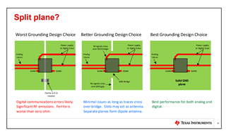
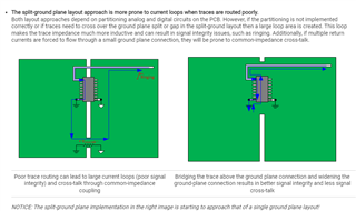
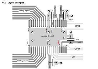
In page no 43: It shows only analog ground , why is digital ground and its connection to IC DGND pin 27 and to analog ground is not addressed?

Is there a specific document for mixed signal layout for this IC other than the datasheet? I could only find a general pcb guideline which I found in this link: e2e.ti.com/.../faq-pcb-layout-guidelines-and-grounding-recommendations-for-high-resolution-adcs

Thank you.

Regards,
May

  • May,

    To answer your question, we generally recommend connecting both digital and analog ground to a common plane.  When I look at the ADS79xx data sheet, I see the recommendations for layout on page 52 and 53 (fig 69 & 70).  Are we looking at the same document?  In any case, if you look at figure 69, you can see that BGND is connected to the ground plane.  In old literature you may see a split plane approach where analog and digital GND are separated and connected at one point.  This approach is typically not recommended in modern literature, and measured results show that one continuous GND plane is best.  I hope this helps.

    We have a detailed video series on the subject.  The series can be found on TI.com and on Youtube.  Below are the links for TI.com.  The series focus is mixed signal systems similar to what would be required for the ADS7951.

    Introduction to PCB design for Good EMC

    PCB Trace as a Wave Guide

    PCB Stack-Up Impact on Performance

    PCB Trace Impedance Matching

    Crosstalk on PCB Layouts

    Data Integrity Issues

    Decoupling Capacitors PCB Layouts

    EMC Compliance Testing Methods and Standards

    Art

  • Hi Art,

    Thank you for the information, my customer have follow up questions, please see details below.

    1. It seems measurements were taken on single a2d , how these are expected to change for multiple a2d based circuits where the currents would much higher?
    2. Were a separate digital ground created at all ? or only one analog ground used to which digital and analog circuits connected ?
    3. The question does not answer how to connect analog and digital grounds if the circuit layout is already with two separate planes.
    4. The layout recommended on page 43 of datasheet does not meet any of the layout presented in your literature, why ?

    Also your literature shows current flowing between the two ground planes.

    Idea is not let much current flow between two ground planes and just join them to create common reference potential. This can be achieved by split planes and having some impedance between them.

    Thank you.

    Regards,
    May

  • May,

    1. It seems measurements were taken on single a2d , how these are expected to change for multiple a2d based circuits where the currents would much higher? Answer:  Each similar device added will increase the digital currents proportionately.  However, the vast majority of the current will flow directly beneath the digital trace.  This means that with good "floor planning" (i.e. keeping sensitive analog away from the digital), the digital return current will have little impact on analog performance.  That is, the current will be contained beneath each digital trace.  See Crosstalk on PCB Layouts for a discussion of current distribution beneath a PCB trace.
    2. Were a separate digital ground created at all ? or only one analog ground used to which digital and analog circuits connected ?  Answer: In general, we recommend one solid GND plane where both digital and analog grounds connect to.
    3. The question does not answer how to connect analog and digital grounds if the circuit layout is already with two separate planes.  Answer: Using two different plans is generally not recommended.  This is especially true if digital signal cross over the split between the two planes.  Driving a digital across a break in a plane can cause RF emissions, substantial crosstalk, and interference with the sensitive analog.  Slide 6, 7, and 8 in Crosstalk on PCB Layouts gives  measured results for digital signals crossing over a split in the ground plane.  If you require a split GND plane, than the best way to do the layout is to create a bridge for any signals that move from the analog to digital sections.
    4. The layout recommended on page 43 of datasheet does not meet any of the layout presented in your literature, why?  Answer: The data sheet is showing the top component layer.  The analog ground copper fill area shown is on the top layer.  The data sheet says:  A copper fill area underneath the device ties the AGND, BDGND, AINM, and REFM pins together. This copper fill area must also be connected to the analog ground plane of the PCB using at least four vias.  The data sheet does not specify if the "ground plane" is solid or split.  It should state solid.  If you choose to use a split plane, the most important thing you should do is to make sure that the SPI signal do not cross over the split.
    5. Regarding your figure.  I agree with the good vs bad layout.  In the case of the good layout, the digital signals cross a ground bridge.  I do not agree with the idea that using the split will improve your performance when compared to a solid plane.  This is mainly true as the return currents will be confined under the signal trace.  I understand that you are skeptical on this subject, and in the past the idea of using a split plane for mixed signal systems was common.  I have used split planes in the past.  However, at this point most EMC experts and most mixed signal designers advocate the use of a solid plane for mixed signal systems.  Split planes are still useful for systems such as motor control and switched supplies that have very high di/dt.  If you use a split, but follow the bridge method in the picture you should be ok.
    6. One last note regarding layout principles.  There is a lot of contradictory information on the web.  Especially older generation document may suboptimal recommendations.  I put together the material in the video series by reading experts such as: Henry Ott, Rick Hartley, and Eric Bogatin.  Here is a link to good videos on split vs solid: https://www.youtube.com/watch?v=vALt6Sd9vlY 

    I hope this is helpful to you.  Let me know if you have questions.

    Art

  • Hi Art,

    Thank you the information, customer have follow up questions. 

    Were a separate digital ground created at all ? or only one analog ground used to which digital and analog circuits connected ?  Answer: In general, we recommend one solid GND plane where both digital and analog grounds connect to.

    In this case should it better to

    1. Connect pin 27 to AGND
    2. Connect pin 27 to DGND
    3. Or create pin 27 to both through zero ohm resistors and keep an option to see what works better in practice?


    1. Lastly , why is your datasheet does not make it explicit that there are two digital and analog grounds and are connected to common ground plane?

    Thank you.

    Regards,
    May

  • May,

    The data sheet shows the analog and digital grounds connected to a common ground pour (see annotated figure below).  The ground pour is called "analog ground" but more correctly should just be called ground.  The data sheet says that this copper fill area must also be connected to the analog ground plane of the PCB using at least four vias.  Pin 27 on the 30 pin TSSOP is BGND (this is the digital ground).  I recommend a solid ground plane, so this pin would simply connect to the ground plane.  If you split the ground plane (not recommended), than this pin should connect to digital ground.   Ultimately, the split plane will need to be connected together on at least at one point.  To answer your last question about our data sheet. The viewpoint on if a solid ground plan or split ground plane is best for mixed signal systems is has changed over the years.  The approach of splitting the planes was common in the past, but now the predominate view point is that the plane should be solid.  This view is supported by EMC experts such as Rick Hartley.  Here is a link to a good video on split vs solid: https://www.youtube.com/watch?v=vALt6Sd9vlY .  In short, some of our older data sheets advocate methods that are suboptimal.  I will mention that this data sheet does not advocate a split plane, but does not explicitly say that one solid GND plane is best.  For your design you will have to solid or split according to your best judgment.  If you choose split just make sure that any trace that moves from the digital section to the analog section moves across a ground bridge and not a split.

    Best regards, Art

  • Hi Art,

    Thank you for the detailed information, my customer suggested that it best if the datasheet will be updated with some of clarifications in this communication.

    Thank you.

    Regards,
    May

  • Happy to help.  Suggestion noted.

    Art