This thread has been locked.

If you have a related question, please click the "Ask a related question" button in the top right corner. The newly created question will be automatically linked to this question.

ADS1278EVM-PDK: Interface ADS1278EVM standalone with SPI Interface

Part Number: ADS1278EVM-PDK
Other Parts Discussed in Thread: ADS1278, , ADS1178

Hello,

I interfaced to ADS1278 EVM from a Cortex-M4 processor via SPI. I am using the MMB0 to provide power, CLK, and reference voltages to ADS1278EVM. Before I apply power to the MMB0 EVM, I would like to confirm this approach please.

Text highlighted is either a question or I am looking for concurrence. Both are located either in far-right column of a table or located within text indicated with a “•”

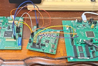
ADS1278EVM is physically removed from the ADS1278EVM-PDK

  • MMB0 is used as a power source to power the ADS1278EVM
  • Used S2 switch to set MODE, FORMAT, and CLKDIV lines, used S1 switch to power all 8 ADC channels, used default S3 switch setting for 27MHz  to clock ADS1278

Below is a visual of what I described above. Tables follow with detail of connections.

S1

All ON (UP)

Power all 8 ADC channels


S2

(SPI, TDM, Dynamic) F0, F1, F2 ALL “OFF”

(MODE [10]) M0 “OFF” M1 “ON”

CLKDIV [0] “OFF”

MODE, FORMAT, and CLKDIV lines


S3

INT (Right)

Using Onboard Oscillator to clock ADS1278EVM

Using buffered on-board

S6

Serial Interface format

FS - Frame Sync format. [1-2], [4-5], [7-8], [10-11]

SPI - SPI-compatible mode. [2-3], [5-6], [8-9], [11-12]

I JUMPED for SPI-compatible mode so,

JP1

Short

FSX IS connected to SYNC/DRDY

I SHORTED this?

JP2

Open

FSR NOT connected to SYNC/DRDY

I OPENED this? UG states only one can be selected

Critical Standalone Connections:

Function

EVM Header/Pin

MMB0

Header/Pin

Cortex-M4

Header/Pin

Pin Name

Description


SCLK

J4.3


SPI2_SCK

CLKX

SCLK

Interface

DIN

J4.11


SPI2_MOSI

DX

Data In


DOUT

J4.13


SPI2_MISO

DR

Data Out


DRDY (SPI)

J4.15


PORTF [10]

INT

DRDY/FSYNC


1.8V

J5.7

J5.7


+1.8VD

Digital supply

Power

3.3V

J5.9

J5.9


+3.3VD

Digital supply


5.0V

J5.3

J5.3


+5VA

Analog supply

Analog Inputs

Channels 1-4

J3.1-8


Analog Inputs


Channels 5-8

J1.3-10


Analog Inputs (ADS1178 and

ADS1278 only)

Ground Connections


DGND

J5.5

J5.5


DGND

Digital ground

Ground

AGND

J5.6

J5.6


AGND

Analog ground input


DGND

J4.4


TP2 GND


Is this the correct BOARD/PIN to hook the Cortex-M4 TP2 GND to?

Voltage Reference

 Reference Voltage

REFN

J3.18

J7.18


Analog Inputs

Reference Voltage

REFP

J3-20

J7.20


Analog Inputs

Analog Inputs

The analog inputs for the ADS1278EVM are connected to J1 and J3. Will connect four devises to Channels J3 1-4 according to sensor datasheet. S4, S5, S7, and S8 default to unbuffered signal.

 Voltage Reference

Switch S3 selects the reference voltage from the buffered REF5025 and is connected to reference pins:

J3.18 = REFN and J3.20 = REFP - supplied by MMB0 motherboard


Mode [1:0]

Mode Selection

CLKDIV

Max fCLK

fMOD

Max fMOD

OSR

fCLK/fDATA

Max fDATA

10

Low-Power

0

13.5MHz

fCLK/1

13.5MHz

64

256

52.734kSPS

Will this work?

Is it safe?

What have I not thought of?

Thanks,

William

  • Hello William,

    I will provide a review for you by end of business tomorrow.  Other customers have successfully used the EVM with their own MCU for code development, so it is definitely feasible.

    Regards,
    Keith Nicholas
    Precision ADC Applications

  • Sounds good Keith. I am completing other functions getting the software ready... But looking forward to you response.

    William

  • Hello William,

    • MMB0 is used as a power source to power the ADS1278EVM
      • Yes, this should work. 
    • Used S2 switch to set MODE, FORMAT, and CLKDIV lines, used S1 switch to power all 8 ADC channels, used default S3 switch setting for 27MHz  to clock ADS1278
      • S3 enables the on-board voltage reference.  Leave it in the default position
    • S1, All ON (UP), Power all 8 ADC channels

      • Yes, this enables all channels
    • S2, ......, MODE, FORMAT, and CLKDIV lines
      • Yes, FORMAT (S2.1, S2.2, and S2.3 all OFF), MODE - Low Power (S2.6 ON, S2.5 OFF), CLKDIV - /256 (S2.4 OFF)
    • S3, right, selects the internal voltage reference, not the local 27MHz oscillator
    • S6, Yes, move jumpers to 2-3, 5-6, 8-9, and 11-12 for SPI mode
    • JP1, JP2 positions do not care since ADS1278EVM is not connected to MMB0 board through J4.  You can leave both of these jumpers OPEN and connect to J4.15 for the DRDY signal.
    • For DOUT pin, suggest connecting to J2.1.  U10/U12 delay the data to meet timing requirements when using frame-sync with the MMB0.
    • DGND, J4.4, MCU ground connection.  Yes, this is probably the best place to connect grounds between the MCU board and ADS1278 board.  You want a good ground return for the SPI lines, and this is where they connect to the ADS1278 board.

    Yes, this setup should work.  The only concern is the wrong power supply connections (your documentation is correct).  Double-check that the AVDD, DVDD, IOVDD, AGND, and DGND pins are properly connected between the ADS1278EVM board and the MMB0 board.  If anything else is incorrectly connected or missing, it should not cause any damage to the board and just require some additional debug.

    Regards,
    Keith

  • Keith,

    This is good information! This confirmation and the suggestions is very helpful.

    This comment below  is what I needed to see. I will apply power as soon as I confirm your recommendations.

    "Yes, this setup should work.  The only concern is the wrong power supply connections (your documentation is correct).  Double-check that the AVDD, DVDD, IOVDD, AGND, and DGND pins are properly connected between the ADS1278EVM board and the MMB0 board.  If anything else is incorrectly connected or missing, it should not cause any damage to the board and just require some additional debug"

    I just have a couple more follow-up questions:

    "Yes, FORMAT (S2.1, S2.2, and S2.3 all OFF), MODE - Low Power (S2.6 ON, S2.5 OFF), CLKDIV - /256 (S2.4 OFF)"

    "S3, right, selects the internal voltage reference, not the local 27MHz oscillator"

    My FORMAT is (S2.4, S2.5, S2.6) M1 is S2.1 and M0 is S2.2 which ones do set... I am inclined to set as you suggested above except for CLKDIV, it appears below that if I want to use 27MHz I have to set CLKDIV as 1...

    So now I am not sure if I have the 27MHz oscillator selected now... Is that by default or do I need to make other setting (see below: If the onboard 27MHz oscillator is selected) to ensure I have the onboard 27MHz oscillator clocking the ADS1278EVM?

    In the SBAU197AUG; Section 5.3 Clock Source

    "The ADS1278 clock can come from one of several sources: the onboard 27MHz crystal oscillator, a clock supplied by a processor on the TOUT pin (J4.17), or an external clock source connected between J4.17(TOUT) and J4.18 (DGND). If the onboard 27MHz oscillator is selected (how do I select it?), the device can be run in high-speed mode, high-resolution mode, low-power mode, or low-speed modes with CLKDIV set to 1If the performance of the device must be explored with CLKDIV set to 0 in the low-power and low-speed modes, an external clock must be provided to the board, either using the TOUT connection or having an external clock source connected to J4.17. The same condition is true if frequencies other than the 27MHz provided by the onboard oscillator must be investigated."

    So I just need to ensure I have the onboard 27MHz oscillator selected and according to the statement above in bold, If the performance of the device must be explored with CLKDIV set to 0 in the low-power and low-speed modes, an external clock must be provided to the board, I will need to set the CLKDIV to 1 instead of 0, I have it set to 0...

  • Hello William,

    Yes, since your are using the 27MHz oscillator, the CLKDIV should actually be set to 1 (S2.4 ON).  I overlooked this when reviewing your questions.

    With the default jumper settings on the board and not plugged into the MMB0 board, the 27MHz oscillator will default to enabled, and provide the required clock for the ADS1278.

    If you want to use CLKDIV 0 mode, then you will need to provide an external clock source of 13.5MHz or lower.  However, this will not effect the performance of the ADC if using CLKDIV 1 and 27MHz or CLKDIV 0 and 13.5MHz; both will operate very similar.

    Regards,
    Keith

  • Thanks again Keith! I will let you know how it goes Sir!

  • Well, I have the EVM POWERED ON… I don’t smell or see smoke Blush

    What I've learned:

    YOU: “For DOUT pin, suggest connecting to J2.1.  U10/U12 delay the data to meet timing requirements when using frame-sync with the MMB0”

     I missed this in the SBAU197A UG. It tells me right there in front of my eyes!!! THANKS!!!

     Chapter 5 ADS1278EVM Hardware Details

    5.5.3 Data Output Signals

    5.5.3.1 DOUT on Digital Interface J4

    In TDM mode, the data from all eight channels can be observed on the DOUT1 pin of the converter. The DOUT1 signal is used by the ADS1x7xEVM-PDK to read back and display all the channels. The digital data output pin on the digital interface header J4 is connected to DOUT1 signal via a D flip-flop. The Dflip-flop provides a half cycle delay in order to align the data correctly to reach the higher speeds of the device. Otherwise, the propagation delay from the MSB in Frame Sync mode may result in missing the MSB out of the data word

     5.5.3.2 DOUTx Header, J2

    All the data output signals (DOUT1 to DOUT8) can be monitored on J2. Table 9 illustrates the pinout for J2.

    Table 9. J2, DOUTx Header

    Data Out

    Pin Number

    Data Out Line

    DOUT1

    1(1)

    2

    DOUT2

    DOUT3

    3

    4

    DOUT4

    DOUT5

    5

    6

    DOUT6

    DOUT7

    7

    8

    DOUT8

    • Pin 1 is top right-hand corner, located next to reference designator.


    Rhetorical Question: SBAU197A UG Section 3 Quick Reference Table 3. Critical Connections; in Function Interface; it states “DOUT J4.13”

    shouldn’t the tech doc writers correct to state “DOUT1 J2.1” since the comment above the Table states:

    “Table 3 provides a quick summary of the connections required for operation of the EVM as a standalone

    YOU: “Yes, FORMAT (S2.1, S2.2, and S2.3 all OFF), MODE - Low Power (S2.6 ON, S2.5 OFF), CLKDIV - /256 (S2.4 OFF)”

    ME: “I am inclined to set as you suggested above except for CLKDIV, it appears below that if I want to use 27MHz I have to set CLKDIV as 1...”

     Yes, I am patting myself on the back... for listening to you!!! I went back to the UG and the schematic supports your settings. THANKS!!!


    Format0 pin32 GPIO2   S2.1

    Format1 pin31 GPIO3   S2.2

    Format2 pin30 GPI04   S2.3

    MODE0  pin34 GPIO0   S2.5

    MODE1  pin33 GPIO1   S2.6

    CLKDIV pin10 CLKDIV S2.4


    The silkscreen on the ADS1278EVM threw me off. I had FORMAT (S2.4, S2.5, S2.6) MODE (S2.1, S2.2) CLKDIV (S2.3). My bad. Should have looked at the schematic!!! Always look at how the hardware engineers have the device pinned out!

    Checking out interface, data acquisition, software functionality now...

    Thanks,

    William

  • Hi William,

    Good luck.  

    Regarding the documentation, we are in the process of updating the EVM, including hardware, software, and documentation.  I do not have a timeline when this will occur, but hopefully when it is finally complete, many of these documentation issues will be cleaned up.

    Have a nice weekend.

    Regards,
    Keith