This thread has been locked.

If you have a related question, please click the "Ask a related question" button in the top right corner. The newly created question will be automatically linked to this question.

DAC8775: DAC 8775 output update rate

Part Number: DAC8775

Dear TI Team,

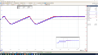
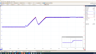
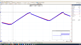
I want to know about the output update rate for four channels in parellel for DAC 8775. It seems it works fine till 1 kHz after that it is not worked properly and I saw some cliiping in signals. 

  • Hi Kishore,

    Lucas will be able to review this and get an answer to you shortly. 

    Best,

    Katlynne Jones 

  • Hi Kishore,

    The typical output slew rate for the DAC8775 is 1 V/µs. What voltage is your reference?

    And just to verify, are you using the configurable slew rate feature? (Bit 4 of Configuration DAC register or on TI's DAC8775EVM GUI)

    Thanks,
    Lucas

  • Hi Lucas and Katlynne,

    Here's some more information:

    The customer is using spi clock 8 MHz, slew rate disabled as VPOS and VNEG are supplied externally and Output enable settings. The problem is that they cannot achieve a data rate more than 1KHz for all four channels.

    The image below shows the channel 1 and 3 comparison.

    The image below is for channels 1 & 4.  the offset with higher frequency like you can see from the picture 1 & 2. The voltage range is configured from 0 to 10V.

    The fall time is always doubled or tripled in case of frequency more than 1 KHz.  the DAC is set up in sequence before the ramp loop and only 3 bytes are transferred for setting the DAC data register. 

    And just to verify, are you using the configurable slew rate feature? (Bit 4 of Configuration DAC register or on TI's DAC8775EVM GUI)

    They are not using the configurable slew rate in Config DAC register. they are writing 0x1001 in the config DAC register (to select output enable and output voltage from 0-10V).

    The customer is enabling the internal reference in reset config register(0x0010) before configuring DAC. After configuring DAC, and selecting the DACs(0x01F0) and Writing into the DACs using internal reference(5V) and  applying +10 to VPOS_IN and -10V to VNEG_IN.

    I hope this helps.

    Regards,

    Marvin

  • Lucas is reviewing this and will respond on monday. 

  • Hi Marvin,

    The externally supplied VPOS_IN and VNEG_IN should have a decent amount of headroom and should be closer to ±13 V.


    These are the expected output rates for the 10 V range (about 12 µs), what output load is the customer using?

    Thanks,
    Lucas

  • Hi Lucas,

    Thank you for the response.

    The externally supplied VPOS_IN and VNEG_IN should have a decent amount of headroom and should be closer to ±13 V.

    The customer have similar problem even for 5v output and always have the problem with update rate.

    In the attachment provided by the customer, you can see that the fall time is also double and offset. They set 250 microsec for update rate that is 4kHz. But the fall time is 500microsec. But for the update rate 1khz is working fine as you can see in the attachments (DAC_5V_1ms).

    Attachement_1385860.zip

    Let me know if you needed more informatoin.

    Regards,

    Marvin

  • Hi Marvin, 

    The datasheet plots use an output load of 1k / 200 pF, what load is the customer using?

    Thanks,
    Lucas

  • Hi Lucas,

    The customer found some extra loads in the schematic that was not present in their original design. Removing those loads resolved the issue.

    Thanks for the support.

    Regards,

    Marvin