This thread has been locked.

If you have a related question, please click the "Ask a related question" button in the top right corner. The newly created question will be automatically linked to this question.

DAC39J84: Multi DAC output synchronization

Part Number: DAC39J84
Other Parts Discussed in Thread: LMK04828

Hi there,

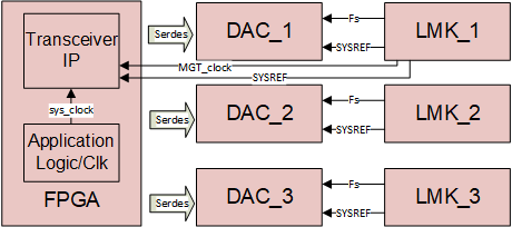
I have multiple DAC39J84 ICs to be synchronized. Each DAC39J84 is clocked by an LMK04828.

In a related thread, ±1 VCO cycle error for LMKs' output device clock aligning was found when performing multiple-LMK synchronization.

Based on this, I found multiple DAC39J84 outputs were not synchronized at the same position after each power cycle, which means I didn't realize the deterministic latency. I am not sure if it is related to the previous LMK sync issue.

The DAC39J84 runs at 1GHz. The JESD204B (subclass 1) parameters are as follows:

L = 8          // Number of lanes
M = 4          // Number of converters per link
F = 1          // Number of octets per frame per lane
S = 1          // Number of converter samples per frame
K = 32         // Number of frames per multiframe
HD = 1         // High Density
N = 16         // Number of bits per sample
N_prime = 16   // Number of adjusted bits per sample

My DAC39J84 register settings are:

(0x00,0x0018)
(0x4a,0xff1e)
(0x01,0x00a0)
(0x02,0x2082)
(0x1a,0x0020)
(0x24,0x0020)
(0x25,0x2000)
(0x3b,0x0800)
(0x3c,0x0228)
(0x3d,0x0088)
(0x3e,0x0108)
(0x3f,0x005a)
(0x4b,0x0700)
(0x4c,0x1f07)
(0x4d,0x0300)
(0x4e,0x0f4f)
(0x51,0x00df)
(0x5c,0x1122)
(0x5f,0x7654)
(0x60,0x3210)
(0x61,0x0001)
(0x4a,0xff1f)
(0x4a,0xff01)

My question is: can we realize the deterministic latency and synchronize multiple DAC39J84 ICs after each power cycle, with the presence of ±1 VCO cycle error for LMK device clock?

I was thinking that the ±1 cycle device clock error was not dominating in the JESD204B protocol, if we can ensure the SYSREF to align LMFCs.

Can you help check if anything is missing in the DAC39J84 register setting?

Thanks and best,

Yilun

  • Hi Yilun,

    As long as DAC sample clock skew between the DACs is less than 1 LMFC window, the DAC sample clock skew will be swallowed by the RBD. The deterministic latency may be affected in an application with low sample rates and high serdes rates. However at 1GSPS, this should not throw off the deterministic latency. However, the DAC output will be 1 code apart. If the +1 clock from the VCO is consistent, the samples for the late DAC can be shifted by 1 at the FPGA.

    Does re-aligning the LMK output divider for these channels not resolve the VCO cycle issue?

    Regards, Chase

  • Hi Chase,

    The LMK synchronization has not been solved. I think the ±1 VCO cycle error of LMK device clock might have an effect here.

    I agree that the SYSREF can be swallowed by the RBD. However, the device clock derives the frame clock and LMFC in JESD204B subclass 1. The ±1 VCO cycle error of LMK device clock is not deterministic (I have a statistics, 80% are ±0 VCO cycle error, 20% are ±1 VCO cycle error), which probably means 80% DAC output is good, 20% DAC output is shifted ±1 clock. Do you agree here? Maybe I have to solve the LMK synchronization first?

    Above is the RX side in DAC chip of JESD204B. I have another question about the TX side in FPGA of JESD204B. Let us say I have 3 DAC39J84 ICs (a,b,c), which are clocked by 3 LMK04828 ICs (a,b,c) respectively. The dclk and sclk can be named as three pairs: dclkout2_a and sdclkout3_a, dclkout2_b and sdclkout3_b, dclkout2_c and sdclkout3_c. When I instantiate three JESD modules (each module for one DAC39J84) in FPGA, shall I use its own dclk and sclk pair (dclkout2_a and sdclkout3_a for DAC39J84_a, dclkout2_b and sdclkout3_b for DAC39J84_b, dclkout2_c and sdclkout3_c for DAC39J84_c), or use one common pair for all the modules (dclkout2_a and sdclkout3_a for DAC39J84_a,dclkout2_a and sdclkout3_a for DAC39J84_b,dclkout2_a and sdclkout3_a for DAC39J84_c), or other combinations?

    Thanks and best,

    Yilun

  • Hi Yilun, kindly see my comments below.

    The ±1 VCO cycle error of LMK device clock is not deterministic (I have a statistics, 80% are ±0 VCO cycle error, 20% are ±1 VCO cycle error), which probably means 80% DAC output is good, 20% DAC output is shifted ±1 clock. Do you agree here?

    Correct, if the VCO cycle error is not consistent then there is no way to guarantee the DAC outputs will be aligned or shifted every power cycle.

    Maybe I have to solve the LMK synchronization first?

    Absolutely. I would suggest to create a new thread with our clocking team to receive faster support on this.

    When I instantiate three JESD modules (each module for one DAC39J84) in FPGA, shall I use its own dclk and sclk pair (dclkout2_a and sdclkout3_a for DAC39J84_a, dclkout2_b and sdclkout3_b for DAC39J84_b, dclkout2_c and sdclkout3_c for DAC39J84_c), or use one common pair for all the modules

    Regarding the FPGA clocking, only a single MGT clock needs to be passed to the FPGA if the serdes are connected on neighboring quads (as typically an MGT clock is capable of being shared to one quad above and below). In this case, the SYSREF can be common.

    If quads are not neighboring, then you will have to pass a second MGT clock (and SYSREF) for that particular quad, etc. But, assuming the LMK outputs are aligned, this should not cause issues.

    If using a Xilinx FPGA, you may be interested in using our TI-JESD204-IP.

    Regards, Chase