This thread has been locked.

If you have a related question, please click the "Ask a related question" button in the top right corner. The newly created question will be automatically linked to this question.

ADS8860: 130MHz BW estimate

Part Number: ADS8860

Hi Team,

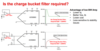
I would like to ask for clarification for this video slide-7, how is it estimated that 130MHz BW is required for op-amp if no charge bucket filter is used?

Here is the video link: training.ti.com/ti-precision-labs-adcs-introduction-sar-adc-front-end-component-selection

I hope you can help.

Regards,

Marvin

  • Marvin,

    The amplifier bandwidth was selected using trial-and-error simulation with amplifiers with different bandwidth.  Beyond helping with amplifier bandwidth requirements, the charge bucket filter helps to minimize noise from the amplifier.  The charge bucket filter is not a true antialiasing filter as its bandwidth is typically beyond the Nyquist frequency of the ADC.  Nevertheless, it does help with some higher order alias signals.  From a practical perspective this kind if filter is used in the vast majority of SAR drive.

    Art 

  • Hi Art,

    I have a follow-up question. I have an ADS8860 interfacing circuit consisting of TLE2142AMD configured as inverting amplifier with gain of -1. There is a 300ohm resistor between the op-amp and ADC. The gain setting resistors are 3.01k and there is a capacitor of 22pF placed across the feedback resistor. Since there is no charge bucket capacitor used in this circuit, can it sample a 5kHz signal varying between 0 to 5V with >=500kSPS sampling rate? SPI frequency is 20MHz.

  • Marvin,

    I ran a simulation and it looks like it does settle to 1/2 LSB according to the circuit you described.  Attached are the simulation results summary in a PDF.  I also show an alternative filer that will minimize the noise and potentially improve settling.  Also attached are the TINA files for the simulation.  Let me know if this answers your question.  Thanks!

    Art

    ads8860 plus tle214x.pdf

    tina simulations ads8860-tle214x.zip  

  • Hi Art,

    I receive a follow-up question:

    "Is there a typo in the 2nd slide? it should be Tacq=2uS-710nS=1.29uS, right?

    Also, as per standard calculation, the minimum acquisition time to get the output settled to 1/2 LSB is 11.78*(300+96)*59pF = 275.2nS. But since its lower than the minimum Tacq specified in datasheet, the minimum acquisition time required is 290nS. Is that correct? So I can go as high as 50MHz SPI frequency, right?
    Note: 96ohm is the resistance of the sampling switch, 59pF is the input sampling capacitance."

    I hope you can explain further.

    Regards,

    Marvin

  • Marvin,

    Yes.  You are correct on the typo.  I should have used 710 for tconv.  This makes it a little more challenging for settling, but you still have a lot of margin.  

    Regarding the standard equation:  This equation is for an RC 1st order system.  The amplifier makes this a higher order system as it's output impedance is not a simple resistance but is complex.  In a previous posting you mention that the sampling rate is above 500kHz.  It doesn't really matter what clock rate you use.  What matters is the sampling rate.  If you run at 500ksps, then the acquisition window is 1.29us (as you calculated).  The acquisition depends on the sampling rate and tconv (tconv is fixed by internal oscillator).  The 1.29us is a fairly long acquisition window.  If you reduce the acquisition window to the minimum (290ns), we should really double check the settling.  I recommend you keep the acquisition window open as long as possible for your application.  This makes it easy to be confidant in your settling.  It also allows to use  the external filter which will improve total noise.  Note that it is possible to have a low  sampling rate and also a higher frequency clock by placing a delay between samples.  Please confirm your sampling rate and I will re-run the simulation.

    Art

  • Hi Art,

    Here's more information:

    Please confirm your sampling rate and I will re-run the simulation.

    The sampling rate is 500kSPS. So, the sampling period is 2uS.

    An a follow up question:

    My understanding is, the last sample converted is sent over SPI during the acquision of the current sample.
    So if I limit the Tacq to 290nS then I need to send out the 16bit data within this 290nS which demands a SPI clock of 55.17MHz? This question is out of academic interest, but I will be limiting the SPI frequency to 20MHz.

    Let me know if you need more information.

    Regards,

    Marvin

  • Marvin,

    You are correct regarding the clock frequency.  The the sampling rate will set the minimum clock frequency.  It is always possible to clock at a higher frequency but still keep the acquisition time longer by leaving idle time to extend the acquisition time.  FYI.  The simulations I sent above are accurate as the conversion time was set to 710ns.  Let me know you have further questions.

    Art