


Hi Team,
Good day! I am posting this in behalf of the customer. Kindly check the full details below.
I'm using the ADS131M03 in a design where I use an STM32 microcontroller to communicate with it via SPI.
When I try to change any configuration writing to the proper register or even just reading the ID register, I don't get the register value as answer in the next communication frame. Instead I get the regular communication frame with [STATUS REG][ADCCh0][ADCCh1][ADCCh2][CRC]. I'm even making sure to clear the ADC buffer with two NULL command readings before sending the command.
In the example below I'm trying to clear the reset flag and change the DRDY signal format to low pulse.
First I send 2 NULL blocks to make sure to clear the ADC Tx buffer.
Then I wait until DRDY is triggered again to send the command 6100h.
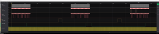
Once the command is sent, I wait until DRDY is triggered again and sent a NULL command to get the answer with the ack from the ADC, but it doesn't send the expected response from a RREG command. Instead it sends the regular STATUS register and the DRDY beahvior doesn't change, which means that I'm not getting to communicate with the ADC properly.
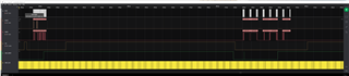
I have tried with different commands and the behavior is the same, not the expected answer.
I also tried first to disable all channels to enable short SPI frames, but no success either.
Thank you in advance for the support.
Best regards,
Jonathan
