This thread has been locked.

If you have a related question, please click the "Ask a related question" button in the top right corner. The newly created question will be automatically linked to this question.

ADC3444: Synchronizing multiple ADCs

Part Number: ADC3444

Hello,

My application requires the capture of samples from four ADC3444s by an FPGA. I have some concerns regarding the synchronicity of the ADCs and whether it will be possible to time correlate the samples.

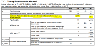
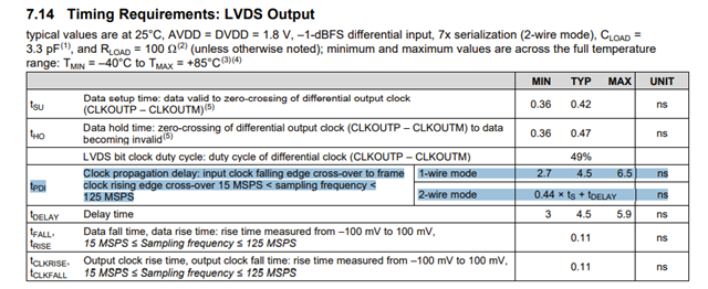
Each of the four ADCs receive the same 125 MHz sampling clock and will run in 2-wire mode. How can I ensure that the conversions of each ADC are synchronized ? Similarly, what's the worst case phase difference among each ADCs DCLKs and FCLKs, and could this make the temporal correlation of samples from each ADC within the FPGA problematic ? Can the SYSREF pin be leveraged in order to ensure synchronicity of the data ?

Thank you. 

  • Hi Adam,

    The ADC3444 has a sync signal that can be used for system synchronization of multiple ADC's. You can use a clocking source that generates a minimum of 4 phase aligned frequencies as the sys ref input. In your custom design, ensure that the trace lengths from the clocking source are matched to eliminate phase errors. 

    Regards, Amy

  • Amy, thanks for your response,

    Perhaps I'm not understanding you correctly. Each of the four ADCs will receive the very same 125 MHz sampling clock. These traces are length matched, so there should be no sampling clock skew between any pair of ADCs. This should synchronize the ADC conversions, but I'm not convinced this will synchronize the LVDS signals of each ADC. Can you clarify what you mean by "you can use a clocking source that generates a minimum of 4 phase aligned frequencies as the sys ref input". Why is a second clock for SYSREF necessary ? Is it not sufficient to simply pulse the SYSREF pin once to synchronize the ADC LVDS signals ? If a second clock is required, what should its frequency be if I intend to sample at the full rate of 125 MSPS ?

    Thanks

  • Hi Adam,

    One option is to use a clocking part that generates multiple phase matched outputs, and these outputs can be used for synchronization. However, what you describe works as well. You can use a single clock for one SYSREF signal, and split it into four independent SYSREF inputs. Just ensure the lengths of the four independent traces are matched.

    Regards, Amy

  • Amy,

    This part has two clock inputs. CLK and SYSREF. CLK is the sampling clock input. This is the signal I'm describing when I said that each of the four ADCs will receive the very same length matched 125 MHz sampling clock. I understand you're discussing the SYSREF input, and that each ADC should also have their SYSREF traces length matched, but I'm trying to understand why this second clock you're describing is necessary for my application. Why do I need a second clock applied to the SYSREF pins of each ADC as opposed to simply applying a single low-high transition to that pin ? 

    For reference, I'm looking at page 50 of this version of the datasheet : ADC344x Quad-Channel, 14-Bit, 25-MSPS to 125-MSPS, Analog-to-Digital Converters datasheet (Rev. B) (ti.com)

    Regards

  • Hi Adam,

    You mentioned that you are providing a 125 MHz sample clock. Do you plan to use the clock divider internal to the ADC3444? The SYSREF signal is designed to synchronize any phase misalignments that may arise from the divider. The application of SYSREF for this part is only needed for synchronization if the clock divider is used for /2 or /4 and you are correct, you can just use a single low-high transition for this. 

    Regards, Amy

  • Amy,

    Thanks for the response. I'm not using the clock divider. I was curious if the SYSREF input is indeed only applicable when the clock divider is used, or if it also corrects phase misalignments among the output FCLK signals of the ADCs, too, but I saw no evidence of this in the datasheet. This brings me back to one of my original questions. 

    What's the worst case phase difference between the FCLK signals of a pair of ADC3444s whose CLK inputs are phase aligned?

  • Hi Adam,

    I now see the confusion with the datasheet; I again read over 9.3.2.1 Using the SYSREF Input (pg. 50). In the diagram under 'TI device' there is no /1 option, only /2 and /4. If you are not using the clock divider, then the clock divider is operating in a 'bypass' ( /1) mode and the SYSREF is not needed. Any phase misalignments would only arise from the input sample clock. 

    Regards, Amy

  • Amy,

    Are you saying there are absolutely no sources of uncertainty internal to the ADCs that can lead to skew between a pair of ADC's FCLKs? What about process variation?

    Regards

  • Adam,

    The only thing which would skew the FCLK is the ADC sample clock plus up to a few hundred ps of aperture delay variation between devices.

    As Amy mentioned, if not using the divide-by-2 or divide-by-4 option within the ADC, then no SYSREF input is necessary. It's a bit confusing having the name SYSREF as this typically refers to system reference for JESD interface devices. In this device, SYSREF reflects what is often referred to in other LVDS devices as a STROBE, often used for aligning the sample clock in higher channel count devices at each internal converter. Anyways, that's aside the point, just hope to clear this nomenclature up a bit since it has caused confusion for some of our customers in the past.

    The only uncertainty within this device will be the aperture skew (aperture delay), which is guaranteed by TI to be less than 150ps in either direction (meaning < 300ps total skew) between any number of devices in a given system. Given that this is a 125MSPS device, the period of one clock is 8ns. This means that the FCLK will be aligned to the same clock edge across all devices (provided that the sample clock is indeed phase aligned). This also means the total variation between FCLK shall be less than 300ps. This should be low enough that the FPGA can swallow this in the receiver as apart of setup/hold timing without any issues.

    The key factor is sample clock alignment and trace length matching for all devices in a system as well as length matching the DCLK and FCLK from each device as well. As the FCLKs will be phase aligned, only one FCLK is required into the FPGA to achieve synchronization, however, many customers will still route the FCLK from all devices to their FPGA as a safety measure.

    Hope this helps clear some things up.

    Regards, Chase

  • Chase,

    Thanks for your response. You have convinced me that a given pair of devices will see no more than a 300 ps delta in their conversion times. However, I'd like to refer you to parameter tpdi in table 7.14 of the datasheet. Maybe I'm interpreting this incorrectly, but it would seem this would also contribute to skew between FCLKs (a worst case of 3.52 ns at 125 MSPS, if I'm understanding this correctly). Can you please confirm If this is true ? 

    Regards, Adam

  • Adam,

    My mistake, you are correct. The datasheet seems to indicate the FCLK may have (worst-case) skew of up to 3.7ns (6.5ns-2.7ns) in 1-wire mode and up to 6.42ns ((0.44*tS (8ns) + Δtdelay (2.9ns)) in the 2-wire mode.

    However, this would indicate a device-to-device variation of up to 3 DCLK periods (or up to 6 bits of data due to DDR) which seems excessive. Please allow us to check with our design team on this. Note that a response may take a while given the holiday week. 

    Regards, Chase

  • Chase,

    Thanks for looking into this. Looking forward to hearing from you after the holidays. Happy Thanksgiving

    Regards, Adam

  • Adam,

    I've had a brief discussion with one of our engineers more familiar with this device. The DCLK is aligned to FCLK to ensure setup/hold timing window. The tPDI value I mention above is incorrect. The FCLK and DCLK will be delayed from the sample clock by a fixed amount 3.5ns (0.44*tS = 8ns)). The actual variation is simply the variation of the delay time, Δ tDELAY, being 5.9ns - 3ns ≅ 2.9ns worst case skew between devices. As this Δ tDELAY is the only variable factor towards Δ tPDI , the Δ tPDI is simply 2.9ns (provided that the input sample clock is in-phase). We do recommend for each FCLK be routed and used for aligning that specific converter's data. My apologies for any confusion earlier. We are trying our best while many engineers are out of office for holiday. Happy thanksgiving to you as well.

    Regards, Chase