This thread has been locked.

If you have a related question, please click the "Ask a related question" button in the top right corner. The newly created question will be automatically linked to this question.

ADS5296A: External Reference circuit BW

Part Number: ADS5296A
Other Parts Discussed in Thread: OPA4353

Datasheet has this note:
"The external amplifier must provide an average current of 5 mA or less at the maximum sample rate."

Not sure how to interpret that. Do I need a wide-band amplifier to drive the reference pins?

  • Hi David, 

    The amplifier will have to drive a 1-uF capacitor (without being unstable), be able to provide a max of 5mA average current, and be low-noise. 

    I pulled up the EVM schematics and I see this particular circuit which you can use as a starting point - U31 opamp is OPA4353 which meets all the above requirements. 

    Thanks,

    Karthik

  • Hi David, 

    I see that you have rejected my answer. Can you elaborate on which part is unclear? 

    Regards,

    Karthik

  • I'm wondering about specific condition: at the maximum sample rate.

    How should I consider sample rate when designing the circuit?

    The EVM circuit has a BW ~1.2 MHz, so if sample rate is in fact a consideration it seems ill suited. It also has significant peaking (in simulation) - is the 100p cap supposed to be on the other side of the 5.1 ohm R?

  • Hi David, 

    From my understanding, I think the circuit is correct. Let me reach out to the designer as well to confirm my understanding. I will get back to you with a detailed explanation by 30 Nov. 

    Thanks,

    Karthik

  • Hello Karthik. Have you gotten any feedback from the designer?

  • Hi David, 

    Yes, I did. 

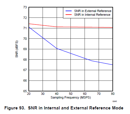
    Firstly, I would recommend for you to use the internal reference circuit. As explained in the datasheet (Figure 93), board and device-packaging parasitics can degrade the SNR performance. Is there a compelling reason why you would want to use the external reference mode? The internal reference circuit gives a gain matching of ±1.5% across devices. 

    In case you do plan to use the external reference mode, to first-order, you can model the load requirement on REFT and REFB as a current impulse every clock edge. The average current drawn for max sampling speed (200MHz) is then 5mA. For a lower sampling speed, the current will scale down linearly.

    Now, for the driver circuit mentioned in this thread above, the impulse current is provided by a big 1uF capacitor and hence the voltage ripple is very small. Also, the DC current to the 1uF capacitor is provided by the opamp. So, a lower closed-loop bandwidth of the driver (opamp + feedback network) is acceptable since it is meant to only provide the DC current.

    Finally, the driver circuit must be stable while driving a 1uF and you might be right on the location of the 100pF. I suggest that you to do a PSPICE simulation using an OPA4353 model here where you can check i) stability of the loop by performing an AC simulation, ii) voltage ripple on the 1uF by modeling REFT/B load currents as a current-impulse-train by performing a transient simulation. 

    Thanks,

    Karthik

  • Thank you, Karthik.

    To your question: our final design will incorporate several devices on a large board with a temperature gradient. We are working on a prototype/proof-of-concept; as part of the effort we plan to evaluate if we need to use an external reference circuit to ensure the voltage reference at each ADC remains within our ability to compensate otherwise.

  • Hi David, 

    Understood. Do reach out if you need any other information. 

    I will close this thread now. 

    Thanks,

    Karthik