This thread has been locked.

If you have a related question, please click the "Ask a related question" button in the top right corner. The newly created question will be automatically linked to this question.

DAC80508: 1)Abnormal SPI communication problem and 2) 2.5V/5V output range

Part Number: DAC80508

Hi team

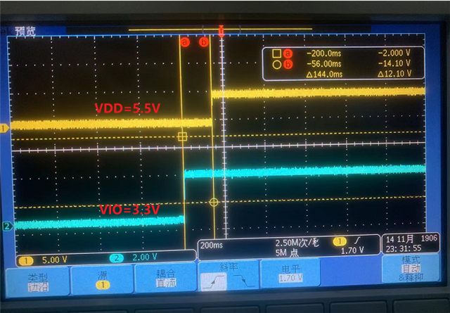
Recently my customer found abnormal SPI communication problem when using DAC80508 and all register readback value is 0x00. 5.5V VDD and 3.3V VIO in this case and you could refer to the attached for the power sequence scope.

5.5V VDD and 3.3V VIO power up sequence:

The customer tried to connected VDD and VIO to the 3.3V power supply and found the SPI communication problem is gone. It is unfortunately that the customer is not able to capture the SPI signals because of the layout.

May I know your comments on this problem? 

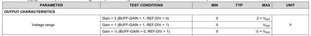
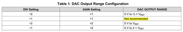
In addition, my customer wants DAC80508 have the 5V and 2.5V FSR range for different channels(2.5V for OUT0~OUT3 and 5V for OUT4~OUT7 for example), but the questions here is that DIV=1 and Gain=1 is not recommended stated in the D/S, the customer also tried this configuration and found 0V voltage for any code. May I know your comments on this? Is it possible to meet this application requirement? 

  • Hi Shawn,

    You mention that the registers are reading back as 0x00, but is the correct voltage seen on the outputs in this case? Please provide the schematic. 

    The DIV=1 and Gain=1 will still work fine. The designer told me it was listed as not recommended to avoid the possible confusion of cases where the supply voltage/ref voltage combination would be problematic. Is VDD 5V during this test? Or are they using the VDD tied to VIO (3.3V)? Can you have the customer try a few different configurations and let me know the output?

    1. Set DIV=1 and Gain=1 for all channels

    2. Set DIV=1 and Gain=2  for all channels

    3. Set DIV=2 and Gain=2  for all channels

    Best,

    Katlynne Jones