Hi Team,
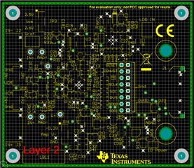
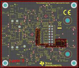
Is it possible to could get the manufacturing gerber files for ADS8900BEVM-PDK? Our customer wants to compare the PCB layout of the ADS8900 IC to their custom layout.
Thanks in advance!
Kind Regards,
Jejomar

-
Ask a related question
What is a related question?A related question is a question created from another question. When the related question is created, it will be automatically linked to the original question.