This thread has been locked.

If you have a related question, please click the "Ask a related question" button in the top right corner. The newly created question will be automatically linked to this question.

ADS1675: For maximising of effective number of bits

Part Number: ADS1675
Other Parts Discussed in Thread: THS4503, THS4551

Hi Texas,


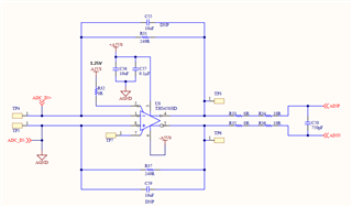
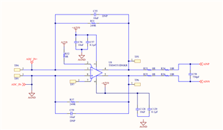
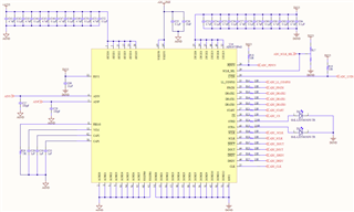
I want to measure the precision voltage (Transimpedance amplifier output voltage, 10kHz-400KHz) with a minimum resolution of 400 uV from the ADS1675. We implemented the attached schematic on PCB (ADS1675REF Eval board) with THS4503 FDA; however, we are not getting desired resolution (30 mV oscillations we are getting). Could you please correct and modify the following points for the next PCB design to achieve a minimum noise floor with ADS1675?

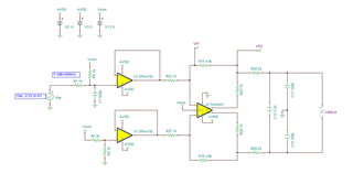
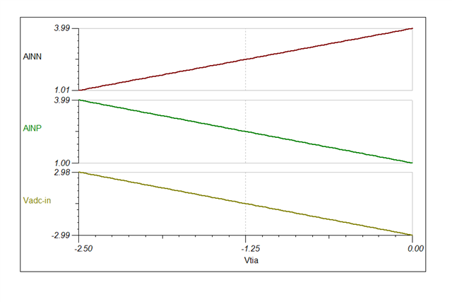
  1. Since the Total output noise from TIA Opamp (Low pass filter at the output node) is 1uV to 2.5 uV. The output of TIA is in the negative range of -2.5 to 0 volts with a stable frequency range of 10kHZ to 400 kHz on various frequency gains. How should we effectively cascade the TIA single-ended signal with FDA (THS4503 or THS4551) to preserve maximum signal fidelity?
  2. Should we use a unity gain inverting buffer between TIA and FDA to minimise the level floor? Will it be fine to use Vocm of FDA to level shift the negative single-ended TIA output signal to feed to unipolar differential ADC i.e., ADS1675?
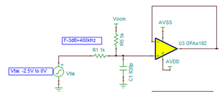
  3. What modifications (not at the cost of signal distortion/loss, noise increment) should we make in the FDA design to utilise the full range of ADS1675 here? TIA output: -2.5 to 0 volt, VrefADC: 3V, AVDD_ADC: 5V.
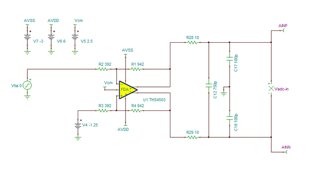
  4. ADS1675 datasheet says (“A 750pF capacitor should be used directly across the analog input pins, AINP and AINN”), placing of this capacitor in THS4551 simulation (attached) is causing the stability issue (negative phase margin, but no intuition as to what exactly it is.). Could you please correct the design for the said requirement? The choice of THS4551 over THS4503 is good for our measurements for better accuracy, precision, and minimum noise distortion.
  5. The offset voltage of FDA is constant (datasheet range, say max offset of THS4551) for a specific set of operating conditions (temp, Vcom, Vcc, Vss etc.)? or this offset voltage may go dynamically from one measurement to another?

Thanks and Regards,
Deepak

THS4551_Stability_for_review.TSC

  • Hello Deepak,

    I apologize for the late reply; I have been on vacation.

    If I understand your signal chain, you have a TIA, followed by a low-pass RC filter, that then connects to the FDA driving the ADS1675. 

    1. Below is a proposed signal chain approach to convert the TIA output voltage from -2.5V to 0V to the full scale +/-3V input range of the ADS1675.

    2. and 3.  The THS4551 amplifier should provide very good performance, but since it is intended to operate from a single 5V power supply, it cannot directly translate -2.5V to 0V input to the necessary differential output voltage of +/-3V with +2.5V common mode.  Level shifting the TIA output voltage to a positive input range will meet these requirements.  Adding Vocm=2.5V to the TIA output as shown in the below drawing will translate the TIA output to 0V to +1.25V.

    4.  The 750pF capacitor was chosen to optimize performance using the THS4503 amplifier.  The above suggested circuit using the THS4551 uses 22ohm output resistors and a 2.2nF capacitor.  This design will be stable and has been shown to provide good performance on similar ADCs.

    5.  The offset voltage will remain stable over the input voltage range.  The offset voltage will only change due to external factors, such as temperature and over time.  However, the supply voltages should be regulated and low noise, as the PSRR of the device will translate changes in supply voltage to additional errors.

    Regarding the attached THS4551 circuit, the output resistors should be increased to improve stability.  In addition, the 80pF feedback capacitors will also reduce phase margin without additional compensation.  I recommend using the output filter and the input filter between the TIA and the THS4551 to provide additional noise filtering instead of the feedback capacitors.  If you need additional filtering, then follow Figure 10-11 in the THS4551 datasheet for a good filter design.

    Regards,
    Keith Nicholas
    Precision ADC Applications

  • Hi Keith

    Thanks for the detailed clarifications. I have some follow-up questions:

    1. Due to the device constraints, the Non-inverting terminal cannot be pulled to the positive output voltage. So, the only possible option we have is to feed -2.5 to 0 volts to ADC. Introducing multiple parts in the signal chain often contributes to noise and distortion hence we want to minimize the number of stages (say inverting opamp which you mentioned in the last reply) Will you please suggest any alternative part which outperforms the THS4053 in terms of single-ended negative signal to unipolar differential output?
    2. You mentioned “ADS1675 the full-scale +/-3V input range”… from the datasheet I found this part is a unipolar ADC that has a range from 0 to 3V. Say if it has a +/-3V input range then why do not we bypass the FDA and directly connect the TIA (-2.5 to 0) with ADC ( AINP=0, AINN =-2.5)?

    Thanks

    Deepak

  • Hello Deepak,

    In order to use a single stage amplifier, you will need to use a wider supply voltage amplifier for the FDA, such as the THS4503.  Below is an example design using the THS4503 (same amplifier suggested in the ADS1675 datasheet).  This circuit will translate -2.5V to 0V at the input to +/-3V differential (+2.5V common mode) at the ADC inputs.

    Please note that both the inputs for the TIA amplifier and the bias voltage (V4=-1.25V) are low impedance inputs (392ohm) and must be driven by low impedance sources.  If the source impedance is more than a few ohms, then both of the differential inputs (R2 and R3) will need to be buffered by a high input impedance amplifier.

    Regarding your second question, the ADC inputs must always be a positive voltage relative to the ADC ground.  As you can see from the above plot, AINN and AINP range from 1V to 4V, but the difference will range from -3V to +3V.

    Vdiff=+3V, AINN=+1V, AINP=+4V, Vdiff=(AINP-AINN)=(4-1)=+3V

    Vdiff=-3V, AINN=+4V, AINP=+1V, Vdiff=(AINP-AINN)=(1-4)=-3V

    Regards,
    Keith