Other Parts Discussed in Thread: SN74AXC4T774
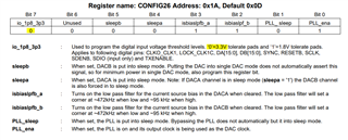
There's no information in the datasheet for default values for the CMOS IO threshold values. I'm looking to interface this DAC with a 1.8V IO FPGA bank
There's no information in the datasheet for default values for the CMOS IO threshold values. I'm looking to interface this DAC with a 1.8V IO FPGA bank