


Other Parts Discussed in Thread: ADS1292R, ADS1292
Hi.
I am developing using ADS1291 and nRF52832.
I have a question about CLOCK settings and data noise.
First of all, my circuit diagram and ADDR settings.
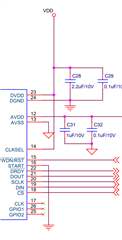
- CLKSEL = 1, AVDD = 5V, I don't use a CLK pin
- Only use the SCLK pin, However, SCLK is SPI Clock, I know that it is not involved in chip clock(right?)
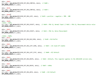
Q1. If CLKSEL PIN = 1, CONFIG2.CLK_EN BIT = 1, CLOCK SOURCE & CLK PIN STATUS both use an internal clock oscillator It's out there.
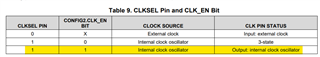
So basically, do you mean that the internal clock can be supported up to 128KHz?
Then, is the DATA RATE value set by CONFIG1.DR2~DR0 applied?
Ex. CONFIG1 = 0x02(500SPS) = 500Hz
15000 data at 30 second measurement
If the above is correct, I don't know what role CLK_DIV plays.
Q2. Does it make a lot of noise when measuring data?
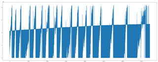
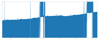
There's too much noise on the data like in the picture, and I don't know why
Thank you.
