This thread has been locked.

If you have a related question, please click the "Ask a related question" button in the top right corner. The newly created question will be automatically linked to this question.

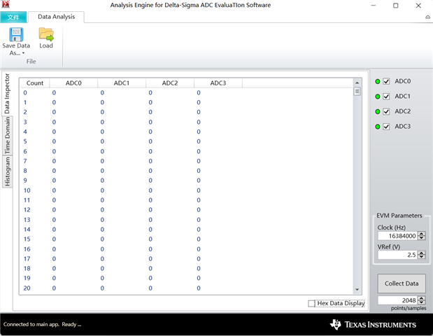
ADS131A04EVM: All the sampling data are 0

Part Number: ADS131A04EVM

Hi Team,

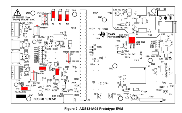
The version of the evaluation board is ADS131A04EVM REV-A, not the latest version from the official website. Software used is Delta-Sigma ADC EvaluaTIon Software, and the computer system is window 10.

According to the user manual, the hardware and software are configured, and communication works. But no matter what voltage is connected to the ADC input pin, the collected data is 0. I'm sure that the power supply is ok, and the registers are also defaulted according to the user manual. The entire evaluation board analog power supply AVDD is 3.3V and AVSS is 0V

IOVDD is 3.3V and ref is 2.5V. Voltage is ok.

After the software communication, I only did the following things:

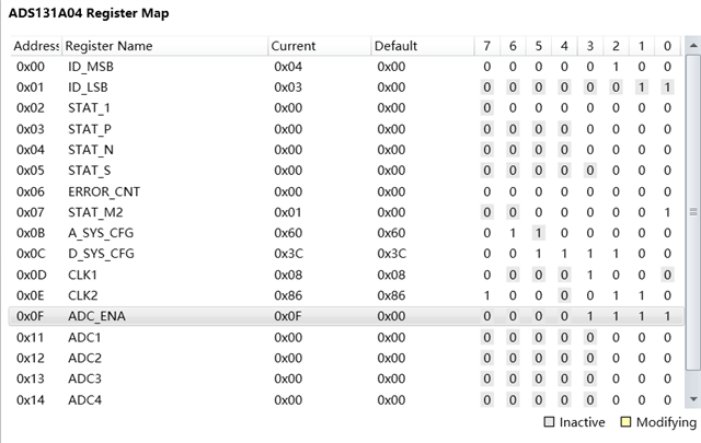
1. Send the command 'unlock' in the software

2. Enable the register ADC_ENA to 1, and all ADC channels are enabled
Kind regards,

Katherine

  • Hi Team,

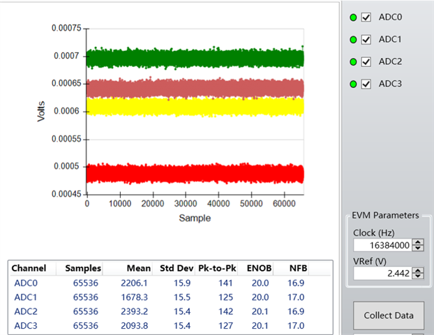
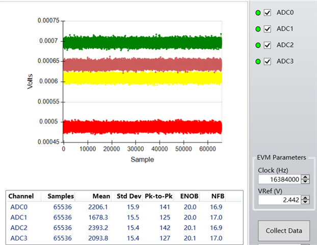
    I want to collect the input referred noise according to the datasheets. The registers and hardware have been set according to the conditions of the specifications. The data collected through the evaluation board are as follows. Is the value of this input referred noise equal to the PT-to-PT value converted to voltage as show in the figure below? Or is it the voltage value shown in the figure?

    If it is the voltage value shown in the figure, the 600uV of the noise would be too much more different from the 15uV shown in the datasheet.

    Kind regards,

    Katherine

  • Hi Team,

    I want to collect the input referred noise according to the datasheets. The registers and hardware have been set according to the conditions of the specifications. The data collected through the evaluation board are as follows. Is the value of this input referred noise equal to the PT-to-PT value converted to voltage as show in the figure below? Or is it the voltage value shown in the figure?

    If it is the voltage value shown in the figure, the 600uV of the noise would be too much more different from the 15uV shown in the datasheet.

    Kind regards,

    Katherine

  • Hello Katherine,

    I apologized for my late response because of holidays in the US. It seems that you were able to capture the data in the GUI.

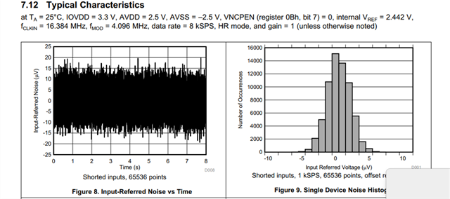
    The graph in the figure 8 shows the input-referred noise and it does not include an offset. According to the data you got in the GUI, the noise can be calculated as below:

    • Your gain=1, Vref=2.442V
    • LSB=FSR/2^24=2*2.442/2^24=0.29uV
    • Vrms_noise=σ_adc*LSB=15.9*0.29=4.6uV
    • Vp-p_noise=6*Vrms_noise=6*4.6=27.6uV

    This peak-peak noise you got matches the noise in the figure 8. 

    You are using the default configuration in the CLK1 and CLK2 registers and the frequency of the crystal on your board is 16.384MHz, so the modulator frequency (fmod) is 1(6.384MHz/8)/8=256kHz according to your configuration in the CLK1 and CLK2 registers. Your data rate is fmod/400=0.64kHz because your OSR is 400 by default, however the datasheet does not have the rms noise data at this data rate. I would suggest you to change the CLK_DIV[2:0] in the CLK1 register from default 100 to 001, and also change the ICLK_DIV[2:0] in the CLK2 register from default 100 to 001,so you will get 4.096MHz fmod frequency. You can collect data in your GUI again and use the same equations above to calculate the rms noise voltage, then you can compare your calculated value with the rms noise data in the table 1 which is highlighted below:

    BTW: The graph you got in time domain of your GUI include an offset.

    Best regards,

    Dale