


The market continues to demand size reduction in various consumer and portable electronics while also to decrease cost in effort to make electronics more affordable. Texas Instruments` DACx3204W and DACx3004W families are the answer to those demands. These devices are one of the smallest quad-channel, 10-bit and 12-bit general purpose DACs (1.8mm x 1.8mm) on the market with voltage and current output capabilities. The small size is achieved through utilizing Die Size Ball Grid Array (DSBGA), also called Wafer-level Chip-Scale Package (WCSP), where leads are connected directly to the die. However, implementation of such innovation could be limiting for cost-sensitive applications because it significantly increases manufacturing cost through the need of via-in-pad and a multi-layer board. This article describes how to eliminate the need for advanced and costly PCB manufacturing processes by routing the DACx3204W and DACx3004W devices in a similar way to their QFN equivalents.
Device Description
Figure 1 shows a block diagram of the DACx3004W and DACx3204W. These devices have an exposed feedback pin that is connected to the output buffer which can be used for closed loop control or an input for a programmable comparator. Additionally, these devices have a high-Z output by default or when VDD is off, along with EEPROM and digitally controlled slew rate.
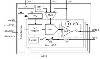
Figure 1. DACx3004W and DACx3204W block diagram
Pinout
Figure 2 shows the dimensions and pinout of the DACx3004W and DACx3204W. To eliminate the need for via-in-pad and a multi-layer board, the output, digital interface, and supply pins are located on the perimeter of the package, while the feedback pins are connected to the four center pins. Such configuration provides easy access to all digital interface pins and analog outputs while limiting the availability of the feedback pins which are not essential to be routed externally for basic DAC operation.
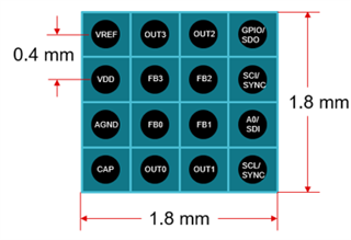
Figure 2. DACx3004W and DACx3204W pinout
Voltage Output
Figure 3 shows a block diagram of a typical voltage out configuration. In order to configure and route the DACx3004W and DACx3204W in voltage output mode, connect the feedback pins to the respective output pins. This can be done on the top layer without adding vias to the feedback pins.
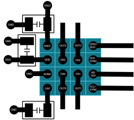
Figure 3. Voltage output configuration
Figure 4 shows a recommended routing example; the trace width is recommended to be half of the pad diameter. This is about 0.1 mm which is still within the range for standard PCB manufacturing processes. The traces can be widened to any width after they leave the outline of the device.

Figure 4. Typical routing for voltage output
Current Output
In order to configure DACx3204W or DACx3004W for current output mode on the PCB, disconnect the feedback pins from the output pins. Figure 5 and Figure 6 show an example block diagram of a typical current mode configuration and a recommended current output routing example respectively.
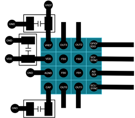
Figure 5. Current output configuration
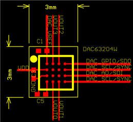
Figure 6. Typical routing for current output
In conclusion, Texas Instruments strives to meet the demand of size reduction and decreased costs from various consumer and portable electronics markets in the effort to make electronics more affordable. While most of the time it is difficult to achieve both size and cost, the DACx3004W and DACx3204W families are able to successfully address manufacturing challenges and make WCSP technology more appealing for cost sensitive applications.
