This thread has been locked.

If you have a related question, please click the "Ask a related question" button in the top right corner. The newly created question will be automatically linked to this question.

LM3S811 control of an ADS8508 16 bit ADC, via the SPI port.

Other Parts Discussed in Thread: ADS8508, LM3S811, ADS8509, LM3S3748


I am failing in my effort to enable a LM3S811 to control an ADS8508 (EVM) 16 bit ADC, via the SPI port.
The object is to trigger and take a reading from the ADC, as required under program control.
I am using CCS Ver: 4.2.3.00004 and the Stellaris® Peripheral Driver Library.
Here are the hardware settings and program listings that I use.
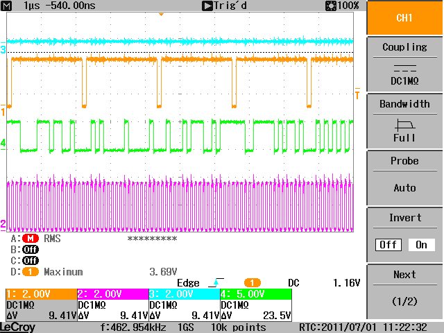
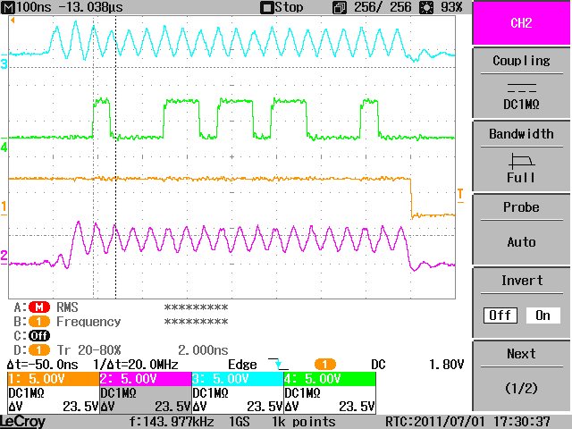
readADS8509(), is called every 2 milliseconds, but the DATA is always high.
Since this is my first attempt at the SSI I could be missing something, or because of the problems
I had with the ADS8508EVM documentation I could have blown the chip.
Any help would be appreciated.

   Earl
  
 //=========================================================================================
ADS8509 I/O
  Inputs:
    TAG      pulled low
    Ext/Int  pulled high
    PWRD     pulled low
    CS       pulled low
    SB/BTC   pulled high
   
    R/C      connected to SSIFss, 1uS every 2mS
    DATACLK  connected to SSIClk, 17 500nS pulses starting on the leading edge of the SSIFss pulse
  Outputs:  
    SYNC     same as the SSIFss pulse
    BUSY     at the trailing edge of SSIFss, goes to ground for 2uS
    DATA     connected to SSIRx, ALWAYS HIGH
 //==========================================================  
void
ConfigSSI(void)
{
    SysCtlPeripheralEnable(SYSCTL_PERIPH_SSI0);   
    SysCtlPeripheralEnable(SYSCTL_PERIPH_GPIOA);   
    GPIOPinTypeSSI(GPIO_PORTA_BASE, GPIO_PIN_5 | GPIO_PIN_4 | GPIO_PIN_3 | GPIO_PIN_2);   
                      
    // Configure and enable the SSI port for TI master mode. 
    //Use SSI0, system clock supply, master mode, 1MHz SSI frequency, and 16-bit data.
    SSIConfigSetExpClk(    SSI0_BASE,
                        SysCtlClockGet(), 
                        SSI_FRF_TI, //data transfer protocol
                        SSI_MODE_MASTER, //mode of operation.
                        1000000, //clock rate
                        16); //number of bits transferred per frame.

    SSIEnable(SSI0_BASE);
}

void
readADS8509(void)
{
    SSIDataPut(SSI0_BASE, 0);

    g_ulADC_In = 10;
    while(SSIDataGetNonBlocking(SSI0_BASE, &g_ulADC))
    {
        ++g_ulADC_In;
    }        
}


  • Hi Earl,

    While we look into your code, can you post a screen shot of your control signals going to the ADS8508?

  • Good morning Tom

      First I goofed! I am using an ADS8509 (16 bit) mounted on an AD8509/8519 EVM board.

    I had written:

        R/C      connected to SSIFss, 1uS every 2mS
        DATACLK  connected to SSIClk, 17 500nS pulses starting on the leading edge of the SSIFss pulse

      Outputs:  
        SYNC     same as the SSIFss pulse
        BUSY     at the trailing edge of SSIFss, goes to ground for 2uS
        DATA     connected to SSIRx, ALWAYS HIGH

    As I started to record the timing signals as you requested I referred to the timing diagram in the data sheet (Figure 3. Basic Conversion Timing (External DATACLK).

    OUCH! I noticed that R/C is inverted.

    I tried using protocols other than SSI_FRF_TI, to no avail.

    They all drive R/C low and enable the data clock, R/C will stay low until after the 17th clock pulse.

    Do I need to add an inverter for SSIFss or create a macro?

      Thank you,

    Earl


  • Hi Earl,

    I have a work-around that seems to be working fine with a LM3S3748. I'm going to clean up the code a little bit and post it as sample code but here are some snippets of the code as it is.

     // Configuration Settings for SSI
     unsigned long ulSCR = 2;                    //Clock Divider parameter for SSI
     unsigned long ulSSIPh = 1;                    //Phase for SSI
     unsigned long ulSSIPo = 0;                    //Polarity for SSI
     unsigned long ulCPSR = 0x02;                //Clock Divider parameter for SSI
     
     unsigned long ulTemp;                        //Temporary variable used for flushing SSI peripheral before starting uDMA
     
    void main(void)
    {
        // Set system clock, use 8MHz Crystal Oscillator on EVB
        SysCtlClockSet(SYSCTL_SYSDIV_4 | SYSCTL_USE_PLL | SYSCTL_OSC_MAIN | SYSCTL_XTAL_8MHZ);
        // Enable SSI peripheral
        enableSSI();
        // Configure the SSI port; master, freescale style SSI, sixteen bit frames
        configSSI(SSI_MASTER, ulCPSR, PROTO_FREESCALESPI, ulSSIPh, ulSSIPo, ulSCR, NINE_BIT_FRAME);
        // Enable uDMA for the SSI Peripheral
        //HWREG(SSI0_BASE + SSI_O_DMACTL) = 0x01;
        while(1)
        {
            writeSSI(0xFF);
            writeSSI(0x1FF);
        }

    }

    I'm using an API I wrote for the SSI0 peripheral (that's where all of the parameters passed to "configSSI()" come from, and the rest of the functions, this API is used in the Stellaris code examples I've posted in the design notes section). I set up the SSI port for 9 bit frames, phase = 1 (I think think phase matters with this device), polarity = 0, and I set the clock divider for the SSI clk to be sufficiently slow such that we're guaranteed that DRDY has pulsed on each acquisition. Your clock divider settings will depend on how your clocking your LM3S811.

    I have MOSI connected to R/C, MISO connected to DATA, SSI0FSS connected to CS, SSI0CLK connected to DATACLK. With the Stellaris SSI peripherals if you don't apply any delay between SSI writes you can actually smash the frames together. So we use two 9 bit frames to create the illusion of a 18 bit frame. The first SSI write gets 0xFF so that we see the appropriate pulse on R/C and the second word is 0x1FF to keep the line high for the rest of the frame. CS goes low for each frame, but since I'm constantly writing CS always stays low.

    Since this interface uses only native features to the Stellaris SSI peripheral you can still use uDMA to collect data, you'll just have to do some massaging on the back end to put the data back together. I'll have to do a little more work to get the data massaged correctly for some nice sample code, I'll let you know when it's posted.


    Blue - CS
    Orange - R/C
    Green - Data out from ADS8509
    Purple - SCLK

  • Earl,

    So I've finally got this interface working, there are some tough challenges to overcome.

    My first attempt above looks good, but on closer inspection I'm actually double requesting on R/C and getting some really strange results.

    So, what I've done is tie CS to ground, increase the SCLK frequency to 25MHz, increased my frames to 10 bit frames (what looks like a 20 bit frame since they're smashed together), and added a delay between each pair of frames. MOSI is still tied to R/C, all the other connections remain the same except CS is grounded. Phase and polarity become important since this interface requires some rigging, Phase = 1, Polarity = 0.

    I'm still getting close to the maximum throughput from the device and I've tied uDMA into the acquisition cycle. You can see a scope shot below, it looks nasty but it works:

    Blue - SCLK
    Green - Data Out
    Yellow - BUSY
    Purple - R/C


    And a screen cap of the resulting waveform:


    And a snippet of the binary data:

    [0] = 0110011011000000
    [1] = 0011011000011011
    [2] = 0011001000011001
    [3] = 0010110111111110
    [4] = 0010100111000101
    [5] = 0010010101111111
    [6] = 0010000100100010
    [7] = 0001110010110110
    [8] = 0001100000110011
    [9] = 0001001110101001
    [10] = 0000111100001110
    [11] = 1011110110101011
    [12] = 1100001101100100
    [13] = 0100101001100100
    [14] = 1110111000111001
    [15] = 1010011111001100
    [16] = 1101111101010100
    [17] = 0000010110110110
    [18] = 0101100100100111
    [19] = 1111011011110100
    [20] = 1010100010010010
    [21] = 1110110010011100
    [22] = 1001111010011100
    [23] = 0000011100100100
    [24] = 1001001010011110
    [25] = 0001011011100001
    [26] = 0011101101010000
    [27] = 0110001100000101
    [28] = 1110110100010000
    [29] = 1000110100110110

    You can see we're actually getting all 16 bits moving in the resulting data, important to note since we have to manually do bit shifting on the data we collect through DMA. I'll be posting the sample code shortly.

  • Greetings Kevin

     Thank you for your efforts, I have also made some progress.

     First, over the years I have become a believer in KISS (KEEP IT SIMPLE) and minimize the variables,

     Also since I am using the 3s811, there is no DMA available and although I have various signal sources I prefer to use a 1.5v battery.

    My test program generates a R/C pulse every 200uS to reads the ADS8509 and outputs the binary reading  as a hex number.

    The SB/BTC pin is grounded and the EXT/INT pin is high.

    I use a GPIO pin to generate the R/C pulse and no connection of SSIClk, SSIfss or SSITx is made to the ADS. SSIRx is conected to a the DATA pin of the ADS.

    Here is the resultant readings, Polarity and magnitude are some what reflective, but the values are confusing.

    Shorted        +1.46v             -1.46v

     ADC=6e    ADC=2584    ADC=db4a   time=0:0:1
     ADC=70    ADC=2586    ADC=db4c   time=0:0:2
     ADC=70    ADC=2586    ADC=db46   time=0:0:3
     ADC=5a    ADC=2586    ADC=db44   time=0:0:4
     ADC=58    ADC=2586    ADC=db46   time=0:0:5
     ADC=72    ADC=2588    ADC=db48   time=0:0:6
     ADC=70    ADC=2586    ADC=db46   time=0:0:7
     ADC=70    ADC=258a    ADC=db48   time=0:0:8
     ADC=70    ADC=2586    ADC=db46   time=0:0:9
     ADC=72    ADC=2584    ADC=db48   time=0:0:10
     ADC=70    ADC=258a    ADC=db46   time=0:0:11
     ADC=5a    ADC=258c    ADC=db46   time=0:0:12

    I need to do a 2's complement of the negative values.

    I will do more after the July 4th weekend. Everyone stay safe.

       Earl

    void
    ConfigSSI(void)
    {
        // enable the SSI0 peripheral
        SysCtlPeripheralEnable(SYSCTL_PERIPH_SSI0);
       
        SysCtlPeripheralEnable(SYSCTL_PERIPH_GPIOA);
        GPIOPinTypeSSI(GPIO_PORTA_BASE, GPIO_PIN_5 | GPIO_PIN_4 | GPIO_PIN_3 | GPIO_PIN_2);   

        SSIConfigSetExpClk(    SSI0_BASE,
                            SysCtlClockGet(), 
                            SSI_FRF_TI, //data transfer protocol
                            SSI_MODE_MASTER, //mode of operation.
                            1000000, //clock rate
                            16); //number of bits transferred per frame. 
        SSIEnable(SSI_BASE);
    }

    void
    readADS8509(void)
    {
        SSIEnable(SSI0_BASE);

        GPIOPinWrite(GPIO_PORTC_BASE, SELECT_ADS8509, 0);
        GPIOPinWrite(GPIO_PORTC_BASE, SELECT_ADS8509, 0);
        GPIOPinWrite(GPIO_PORTC_BASE, SELECT_ADS8509, SELECT_ADS8509);
        SSIDataPut(SSI0_BASE, 0);
       
        while(SSIDataGetNonBlocking(SSI0_BASE, &g_ulADC))
        {
        }
    }