Hello!
I am trying to write and read from registers on DAC70504EVM. I tried to write and then read from DAC0-DATA register (0x08).
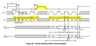
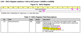
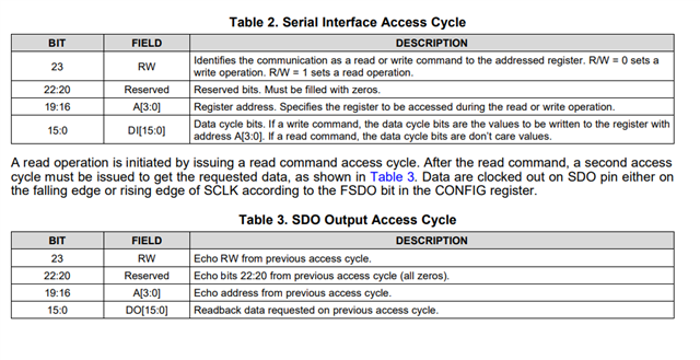
As far as I understand from documentation (sbas871c.pdf), from tables on page 25, it is necessary to send (24-bits long) messages:
First I sent "write" message in order to write 0xEE value in DAC0-DATA register (0x08):
0 000 1000 0000000011101110
Then I was sending "read" messages in order to read respond from SDO:
1 000 1000 0000000000000000
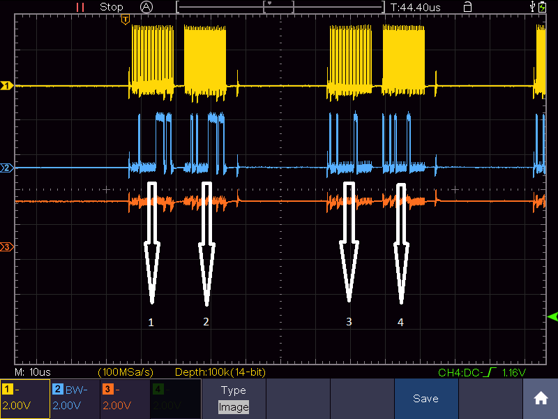
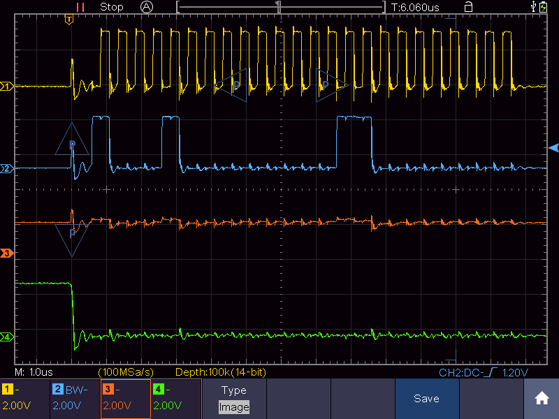
The problem is that SDI pin (orange signal) is high all the time and it is not behaving as expected:

(SCLK - yellow, SDI - blue, SDO - orange, CS - green)
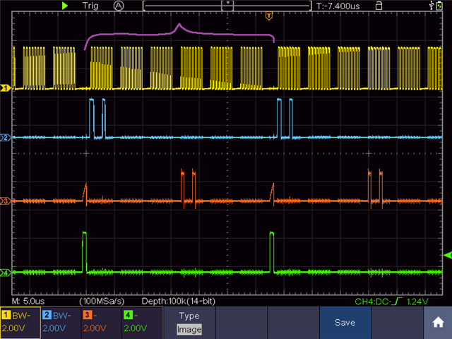
Also, I tried configuration where SCLKs are consecutively, the SDO behaviour is same:
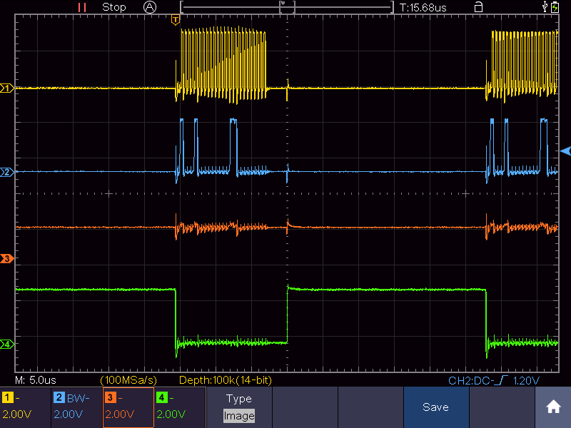
(SCLK - yellow, SDI - blue, SDO - orange, CS - green)
The question is are the messages sent in the right way, and If not what I am doing wrong?
Best regards,
Marko