This thread has been locked.

If you have a related question, please click the "Ask a related question" button in the top right corner. The newly created question will be automatically linked to this question.

ADS1293: No correct data received

Part Number: ADS1293

Hi,

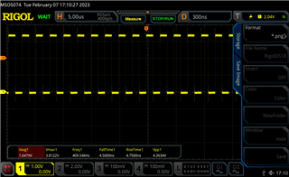
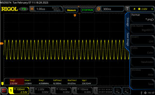
I built a EKG device with the ADS1293 and I have trouble to get correct readings. I can correctly write and read back registers over SPI, so this should not be the issue. I set up the Testing modes for the ADC, but I get only garbage values out of it (random). So I measured all the signals and so far everything looks good (CVREF is perfectly 2.4V), except I'm unsure about the oscillator. The signal seems to have an offset of around 3V and only swings with an amplitude of around 100mV. I tried different load caps but could not really change the behaviour at all, so I think that might be an issue. When I deactivate the external crystal over SPI, I do not get readings at all. 

What amplitude should the XTAL CLK show when running correctly? Might the layout be an issue here (I gave 20mil clearance for the XTAL nets and so far I never had any issues with crystals in microcontroller applications, but I might have removed the GND plane underneath it?

So, is the CLK signal incorrect here (Measured with a x10 Probe):

Edit:

Problem solved, there was a wrong connection from the supply.

  • I could now verify by using the following command, that the XTAL seems to work just fine, at least I get a CLK output matching the frequency of 409.6MHz:

    TI_ADS1293_SPIWriteReg(0x12, 0x05);

    CLK output pin:

    Now from a hardware point of view, everything looks good (SPI working, can Read/Write Registers, Vadc @ 2.4V etc.), but I cannot measure correctly in the test mode. What I'm doing is the following: (Just test Channel 1)

        nrf_delay_ms(1000);
        TI_ADS1293_SPIWriteReg(0x12, 0x05); // internal oscillator, external FB
        nrf_delay_ms(100);
    
        TI_ADS1293_SPIWriteReg(0x01, 0xC0); // Run TST1 --> zero test signal = Vadc/2
        nrf_delay_ms(1);
        TI_ADS1293_SPIWriteReg(0x21, 0x02); // Set Decimation Rate to 5
        nrf_delay_ms(1);
        TI_ADS1293_SPIWriteReg(0x2F, 0x10); // Turn On Channel 1 for loop read back mode
        nrf_delay_ms(1);
        TI_ADS1293_SPIWriteReg(0x27, 0x08); // Assert DRDYB pin Channel 1, ECG
        nrf_delay_ms(1);
        TI_ADS1293_SPIWriteReg(0x00, 0x01); // Starts data conversation
        nrf_delay_ms(1);
    
        while(1)
        {
          if(!nrf_gpio_pin_read(GPIO_ADS1293_DRDYB)) 
          {
              uint8_t temp_buf[3] = {};
    
              TI_ADS1293_SPIReadReg(0x37, buf, sizeof(buf)); // 0x37
              temp_buf[0] = buf[1];
              TI_ADS1293_SPIReadReg(0x38, buf, sizeof(buf));
              temp_buf[1] = buf[1];
              TI_ADS1293_SPIReadReg(0x39, buf, sizeof(buf));
              temp_buf[2] = buf[1];
    
              uint32_t voltage = (((uint32_t) temp_buf[2]) | ((uint32_t) temp_buf[1] << 8) | ((uint32_t) temp_buf[0] << 16));
              NRF_LOG_INFO("Vmes: %d", voltage);
    
              nrf_delay_ms(40);
          }
        }

    Here are some values I get back for zero test:

    <info> app: Vmes: 1628905
    <info> app: Vmes: 1779090
    <info> app: Vmes: 1927419
    <info> app: Vmes: 1664190
    <info> app: Vmes: 2120028
    <info> app: Vmes: 1876972
    <info> app: Vmes: 1254840
    <info> app: Vmes: 1580527
    <info> app: Vmes: 2055585
    <info> app: Vmes: 1772079
    <info> app: Vmes: 1630978
    <info> app: Vmes: 1548289
    <info> app: Vmes: 1464570
    <info> app: Vmes: 2133578

    So this looks not at all near to VADC/2, since ADC is 2^24, it should show more something like 8388608. What am I missing here?

  • hi,

    -------------------------------------------

    What do you mean by "XTAL seems to work just fine, at least I get a CLK output matching the frequency of 409.6MHz:"? 

    Which CLK are you referring to and where did you probe the CLK?

    If you bring the CLK signal out by setting EN_CLKOUT = 1 and probe CLK pin(#21), it should be around 409.6 kHz.

    ----------------------------------------

    Do you have/use a evaluation kit/board(EVM)?

    The best way to verify/validate the design is to compare with the EVM schematic as well as the probe on the TPs on EVM to verify their communication timing diagram.

    -------------------------
    In the meantime, Can you read the REVID: Revision ID register (0x40)

    Revision ID 00000001 (Default)

    Thanks