


Hi team,
One of our customer's issues, I'm forwarding it below, could you please provide some troubleshooting suggestions?
Requirements:
The device input clock uses a differential clock: Input 144MHz,
Use CPLL to generate a sample rate of 720MSPS sample signal.
JESD using mode0, single lane rate 5.76Gbps, 8 lane, data scrambling, sysref signal 2.25MHz
Configuration Process:
First, using the following register configuration sequence and value configuration according to section 9.3 of the datasheet. Read CPLL, SPLL not locked, JESD not issuing sync code.
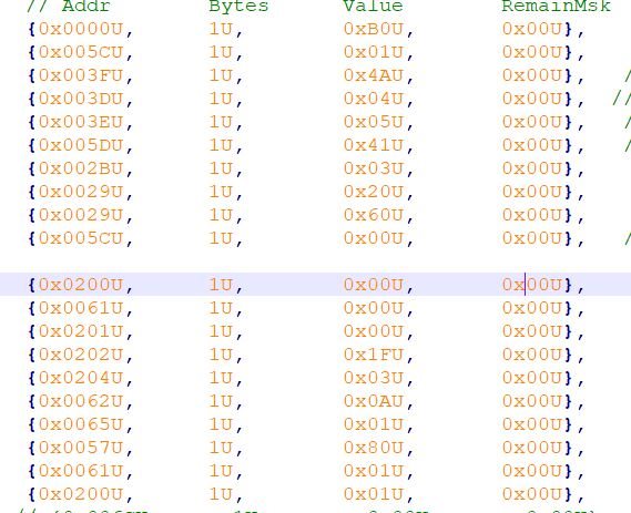
The first column in the figure is the register address, the third column is the register value written, after the 0x00 register is written 0xB0, the 0x270-register is read 0x01,The write continues, and nothing happens after the write completes
Then use the following register configuration table:
{0x00U, 1U, 0xB0U, 0x00U},
{0x02U, 1U, 0x00U, 0x00U},
{0x10U, 1U, 0x00U, 0x00U},
{0x29U, 1U, 0xE0U, 0x00U},
{0x2AU, 1U, 0x00U, 0x00U},
{0x2BU, 1U, 0x03U, 0x00U},
//0X30 0XA000
{0x30U, 1U, 0xA0U, 0x00U},
{0x31U, 1U, 0xA0U, 0x00U},
{0x37U, 1U, 0x4BU, 0x00U},
{0x3BU, 1U, 0x00U, 0x00U},
{0x3CU, 1U, 0x01U, 0x00U},
{0x3DU, 1U, 0x04U, 0x00U},
{0x3EU, 1U, 0x05U, 0x00U},
{0x3FU, 1U, 0x4AU, 0x00U},
{0x48U, 1U, 0x03U, 0x00U},
{0x57U, 1U, 0x00U, 0x00U},
{0x58U, 1U, 0x00U, 0x00U},
{0x59U, 1U, 0x00U, 0x00U},
{0x5CU, 1U, 0x00U, 0x00U},
{0x5DU, 1U, 0x41U, 0x00U},
//0X5E //READ
{0x61U, 1U, 0x01U, 0x00U},
{0x62U, 1U, 0x01U, 0x00U},
{0x65U, 1U, 0x01U, 0x00U},
{0x68U, 1U, 0x61U, 0x00U},
{0x6BU, 1U, 0x00U, 0x00U},
{0x6CU, 1U, 0x01U, 0x00U},
{0x7AU, 1U, 0x00U, 0x00U},
{0x7CU, 1U, 0x00U, 0x00U},
{0x7EU, 1U, 0x00U, 0x00U},
{0x7FU, 1U, 0x00U, 0x00U},
{0x80U, 1U, 0x00U, 0x00U},
{0x81U, 1U, 0x00U, 0x00U},
{0x9AU, 1U, 0x08U, 0x00U},
{0x9BU, 1U, 0x07U, 0x00U},
{0x9DU, 1U, 0x00U, 0x00U},
{0x160U, 1U, 0x00U, 0x00U},
{0x200U, 1U, 0x01U, 0x00U},
{0x201U, 1U, 0x00U, 0x00U},
{0x202U, 1U, 0x1FU, 0x00U},
{0x203U, 1U, 0x01U, 0x00U},
{0x204U, 1U, 0x03U, 0x00U},
{0x205U, 1U, 0x00U, 0x00U},
{0x206U, 1U, 0x00U, 0x00U},
{0x207U, 1U, 0x00U, 0x00U},
// {0x208U, 1U, 0x00U, 0x00U},
{0x209U, 1U, 0x03U, 0x00U},
{0x20FU, 1U, 0x00U, 0x00U},
{0x210U, 1U, 0x03U, 0x00U},
{0x211U, 1U, 0xF2U, 0x00U},
{0x213U, 1U, 0x07U, 0x00U},
//0X270 //READ
{0x29AU, 1U, 0x0FU, 0x00U},
{0x29BU, 1U, 0x04U, 0x00U},
{0x29CU, 1U, 0x1BU, 0x00U},
{0x2C1U, 1U, 0x3FU, 0x00U},
{0x2C2U, 1U, 0x3FU, 0x00U},
{0x2C4U, 1U, 0xFFU, 0x00U},
{0x330U, 1U, 0x00U, 0x00U},
{0x332U, 1U, 0x00U, 0x00U},
{0x334U, 1U, 0x00U, 0x00U},
{0x336U, 1U, 0x00U, 0x00U},
{0x338U, 1U, 0x00U, 0x00U},
{0x33AU, 1U, 0x00U, 0x00U},
{0x33EU, 1U, 0x00U, 0x00U},
{0x360U, 1U, 0x00U, 0x00U},
{0x361U, 1U, 0x00U, 0x00U},
{0x362U, 1U, 0x00U, 0x00U},
{0x363U, 1U, 0x00U, 0x00U},
{0x364U, 1U, 0x00U, 0x00U},
{0x365U, 1U, 0x00U, 0x00U},
{0x366U, 1U, 0x00U, 0x00U},
{0x367U, 1U, 0x00U, 0x00U},
The first column is the address, the third column is the register write value, CPLL SPLL is not locked, no response.
May I know if there is an accurate sequential configuration table of registers?
Best Regards,
Amy Luo

