Other Parts Discussed in Thread: ADS127L11,
Hello,
I have a design using a SAME70Q21 microcontroller with a TI ADS127L11 and TI DAC8832 hooked to the same instance of the SAME70 master SPI peripheral ("SPI1"). This SAME70 SPI peripheral allows up to 4 different SPI slave devices to be hooked to one of 4 chip select instances. Furthermore, the SAME70 SPI peripheral is designed to be configured to allow each of those slave devices to have different SPI CLK phase and polarity behaviors (i.e. SPI clock either idles low or high, data is either clocked out on rising or falling edge of clock). The configuration is called "variable chip select" mode.
This brings me to the two TI Devices on the bus.
The ADS127L11 ADC requires the clock to idle LOW and also requires the data to change state on the RISING edge of SCLK and be read on the SCLK FALLING edge.
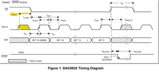
The DAC8832 DAC doesn't explicitly state that the SPI clock should ide high, but it does explicitly state the master micro should have the data change state of the FALLING edge of SCLK. The DAC will then capture the data on the RISING edge of SCLK.

Also of note, the DAC8832 Figure 1 timing diagram seems to show a don't care state of the idle SPI CLK. prior to CS falling. It also calls out a "Tdelay" parameter of 10nS. Am I interpreting this correctly that the DAC8832 doesn't care what state the CLK is in prior to CS falling, only that it must be in that state for AT LEAST 10nS before the CS goes low?

This brings me to what I'm observing with my logic analyzer. My SAME70 micro appears to be handing the multiple slave devices correctly, and their respective CLK idle states. The main concern is the amount of time the micro is providing for that CLK idle level before it starts the CS assertion and subsequent clocking.
For all of these captures, the SPI clock is configured to 1MHz. I'm only able to sample at 50MHz on the analyzer
Here's a capture of the ADWS127L11 ADC:

We can see that the CLK is idling high at the beginning of this capture. This is because the last access done on the SAME70 SPI peripheral was to the DAC8832, who has an active high CLK configuration. After a SPI access is over, SAME70 leaves the CLK in whatever the idle state is for that particular slave peripheral. In the case of the DAC8832, CLK is left high. We can see that as soon as the SAME70 starts to interact with the SPI bus, it yanks the SPI CLK into that new SPI slave device's idle state, which in the case of the ADS127, it LOW. This effectively happens at the same time as CS going low. Then, on the diagram, we see the proper SPI clock data relationship for the ADS127LL, with the ADC changing the state of the data line on the rising edge of CLK, and latching it on the falling edge.
We see the same behavior with the DAC8832. On this capture, the interaction with the ADS127LL just occurred a few milliseconds prior to his analyzer capture, therefore the CLK is idling low. Then when the SAME70 begins to interact with the DAC8832, it yanks the CLK to the DAC8832 required CLK idle state of high, but it does this at pretty much the same time as CS going low. However, we can observe the required timing and behavior being met, with the data line being changed on the FALLING clk edge and data being captured on the RISING CLK edge.

In the end, this appears to be working with both slave peripherals when I run it on the actual hardware. However, I'm concerned I might be "right on the edge" with timing and would like to get feedback from TI if this kind of timing is well within the respective chip timing margins.
Also, while I can adjust many chip select and clock delays on the SAME70, in variable chip select mode, I'm unable to explicitly specify the amount of time the clock idles in an idle state before it tries to asser the chip select.
Thank you very much for looking at this. Please let me know if I can provide further clarification.

