This thread has been locked.

If you have a related question, please click the "Ask a related question" button in the top right corner. The newly created question will be automatically linked to this question.

DAC8728: DAC8728 Gain and offset setting error

Part Number: DAC8728

We are using the TI Part DAC8728.

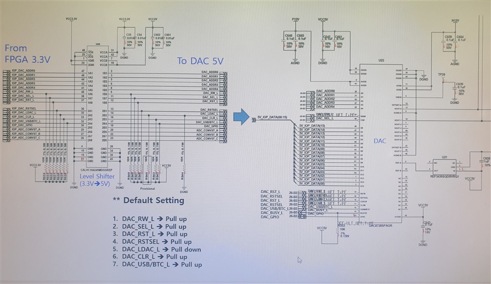
Currently applied DAC8728 Circuit set as below.

1. AVDD +12V, AVSS -12V

2. DVDD +5V

3. IOVDD +5V

4. REF +5V

The desired value does not come out when setting Gain and offset value shown in datasheet. 

( we already have set up power sequence page41 in datasheet.)
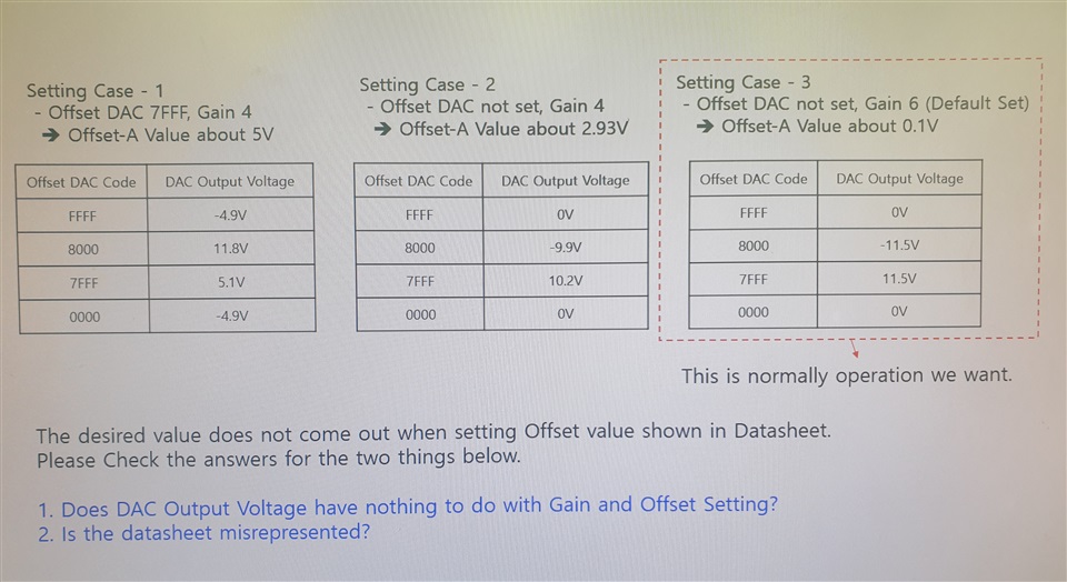
Please Check the answer for the two things below.

1. Does DAC Output Voltage have nothing to do with Gain and Offset setting?

2. Is the datasheet misrepresented? 

  • Hi Woo,

    Could you please upload the schematic you are using for this part so I may see how exactly it is setup?

    Thank you,

    Garrett Shirley

  • Please downloading the image and enlarge it for viewing.

  • Hi Woo,

    Thank you for uploading your schematic. Can you confirm for me that the /USB/BTC pin is not being driven low? That pin must be tied to IOVDD for the DAC code to be treated as a 2's complement value as seen on page 35 of the datasheet.

    To answer your first question, equations 1 and 2 on page 34 of the datasheet show the relation between the DAC gain/input code/offset DAC code and the overall VOUT. The offset DAC can be used to shift the entire transfer function of the main DAC to have an asymmetrical bipolar output. Tables 6 and 7 on page 36 of the datasheet show some example offset DAC codes and the resulting minus and positive full scale outputs of the main DAC. In order to have the outputs you indicate in your setting case 3 you would need to set the offset DAC to code 0x999A, set the gain to be 6, and have the /USB/BTC pin tied to IOVDD for the DAC code to be treated as a 2's complement value.

    Thank you,

    Garrett Shirley